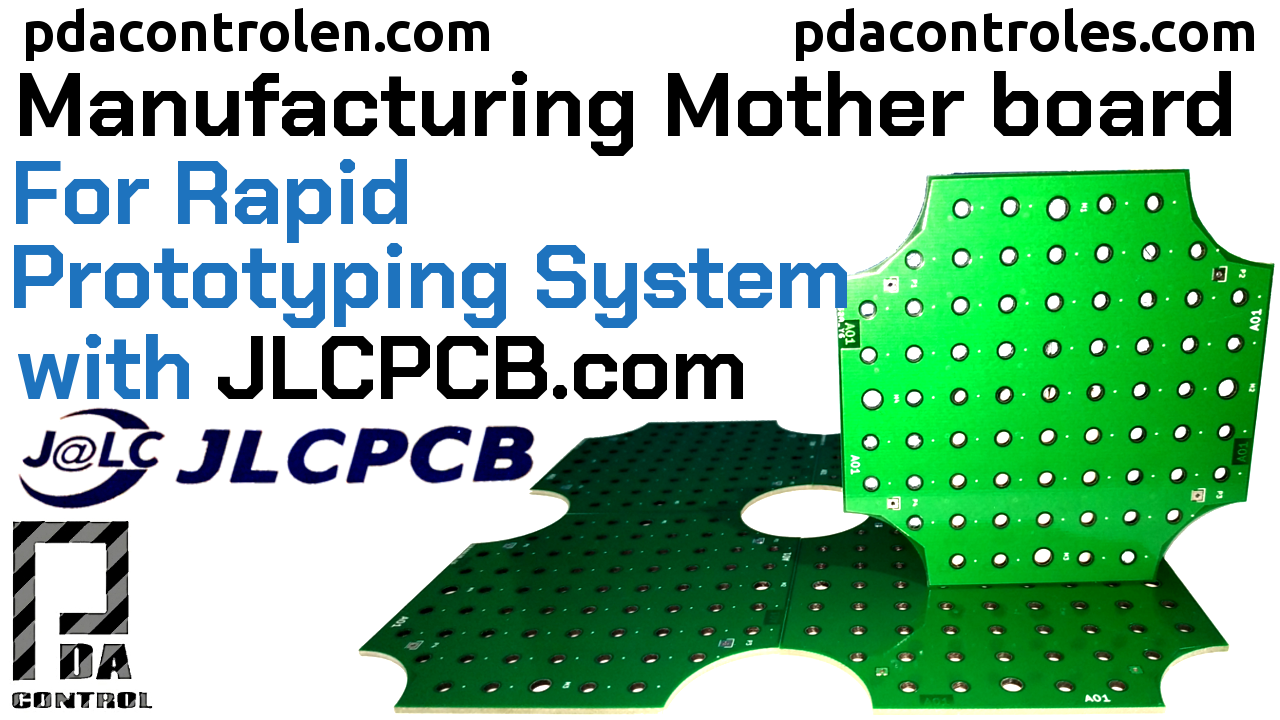
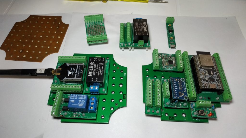
A colleague has designed a rapid prototyping system, mixing practicality with robustness in the assembly of DIY projects, integrating assembly of ESP32 modules, Arduino, Raspberry Pi, Lora I / O ADC, sensors and relays among other peripherals for external assembly.
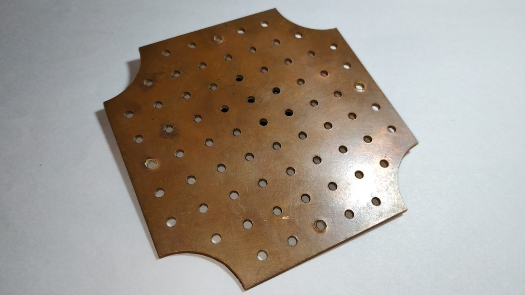
Initially, pcb’s were created in an artisanal way for tests, after tests it has been decided to manufacture in a professional way.
On this occasion I will manufacture the motherboard of our system consisting of many parts, with the help of the manufacturing service of JLCPCB.com I will manufacture some motherboards.
Design in KiCAD
As it is recurring in our channel we will use the opensource KiCAD PCB manufacturing software.
The motherboard was completely designed in KiCAD, my colleague does not need to create a schematic diagram, I manually design the pcb.
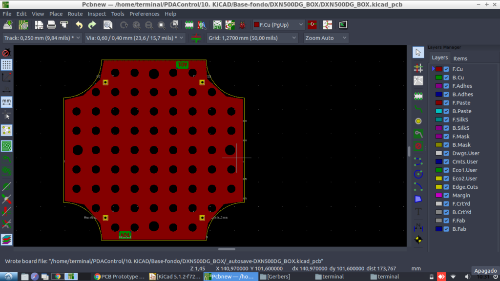
The base has separations, for the assembly of other devices that we will be testing little by little, with the gerber files the revision and manufacturing are carried out.
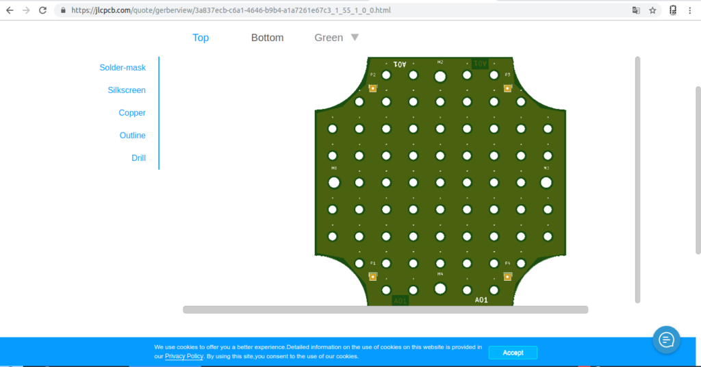
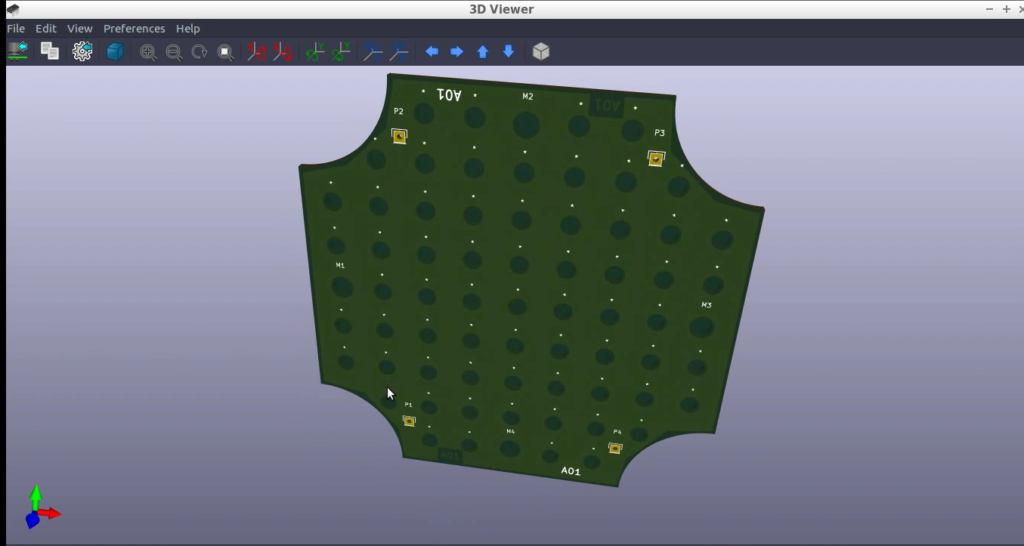
3D preview in KICAD
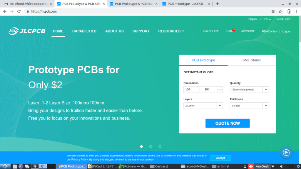
Fabrication at JLCPCB.com
Upload Gerber Files to JLCPCB:
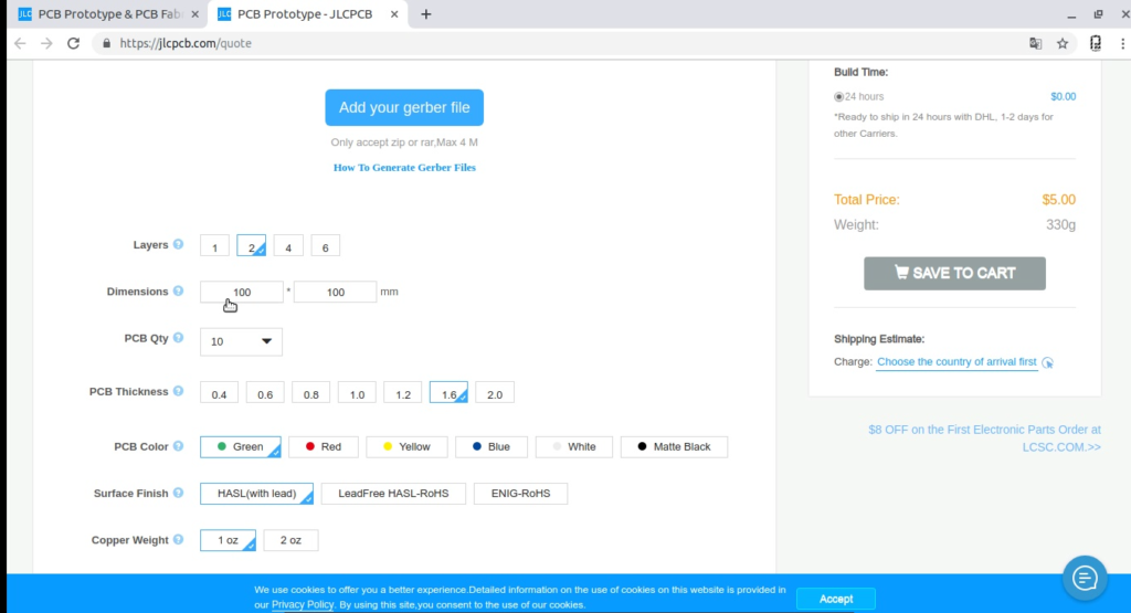
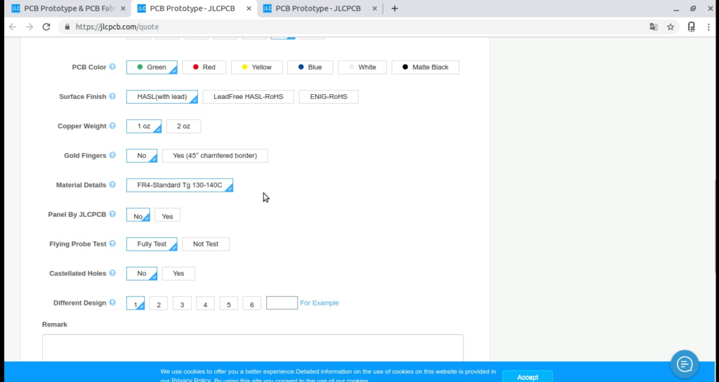
Establish and verify or modify manufacturing parameters:
Verify final design.
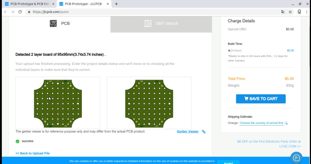
Verify that the order has been loaded correctly.
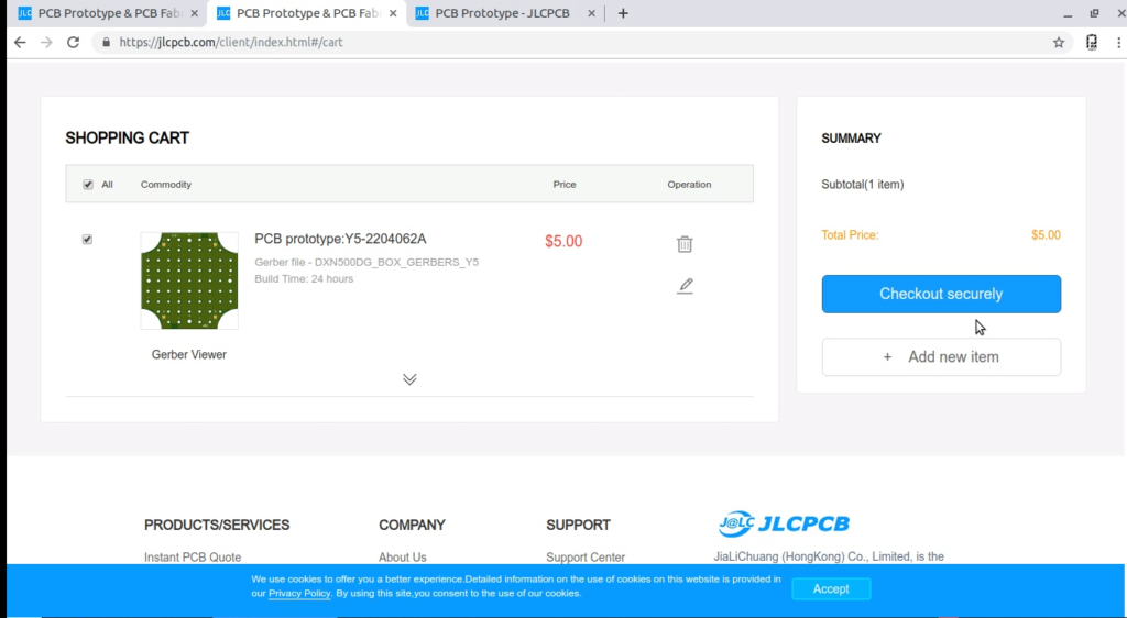
Make payment and enter data for the shipment.
My PCB’s arrived
A few weeks later my PCBs arrived.
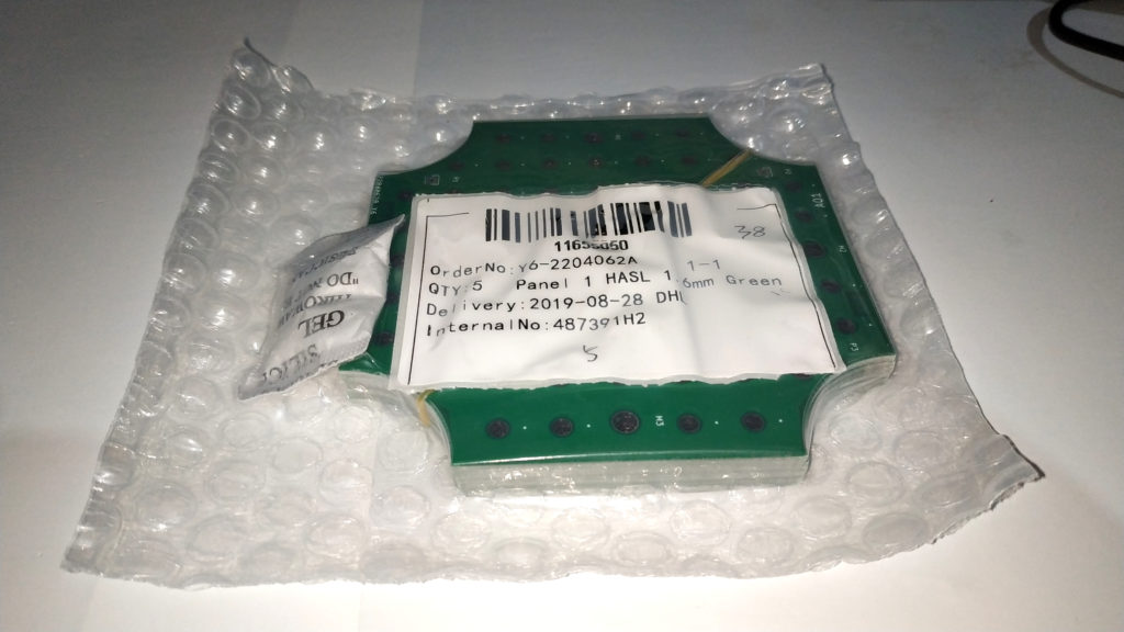
They were perfect !!
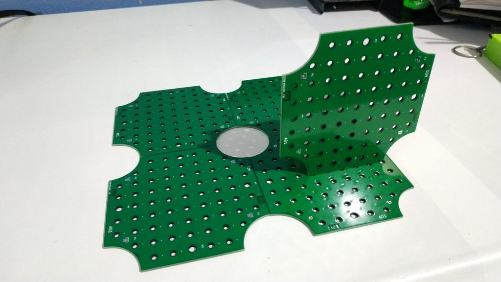
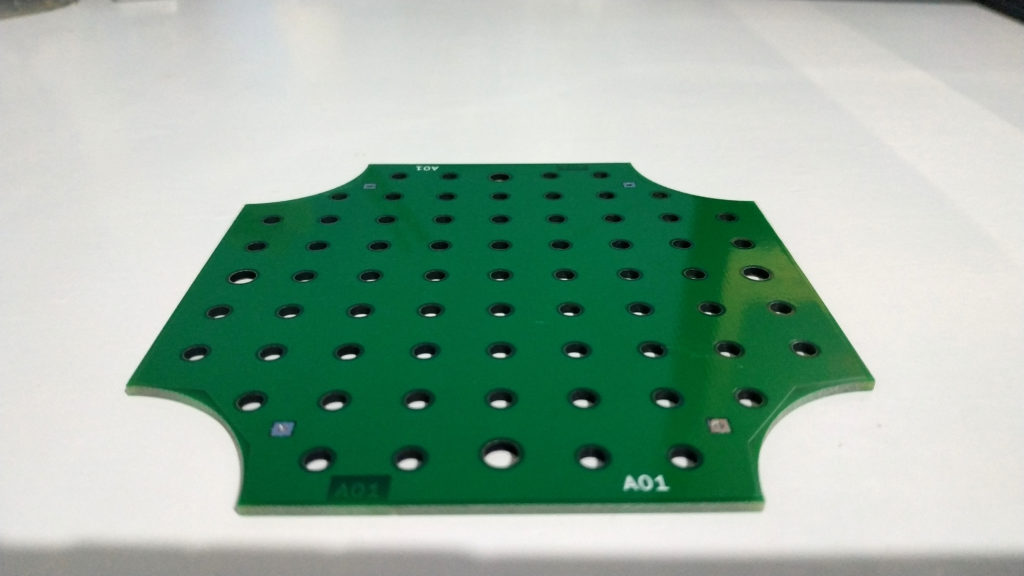

Each plate was designed to mount in a small Dexson cabinet.
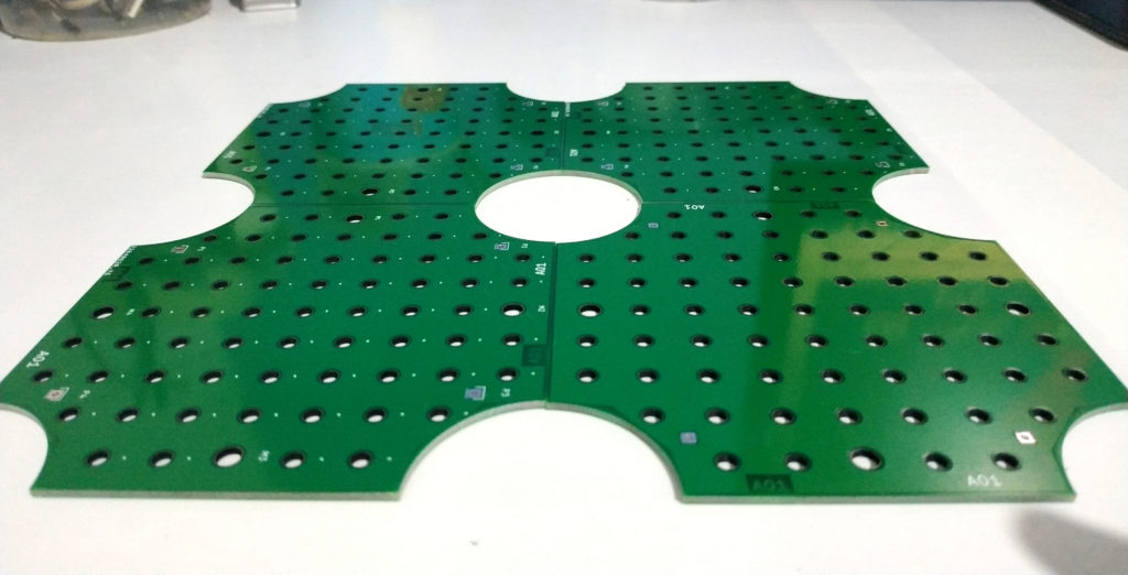
Rapid Prototyping System
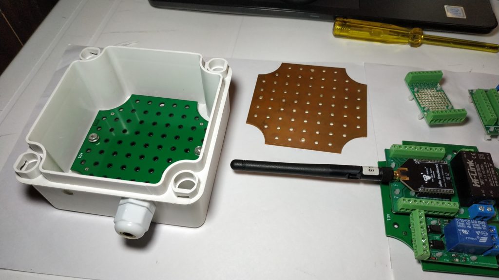
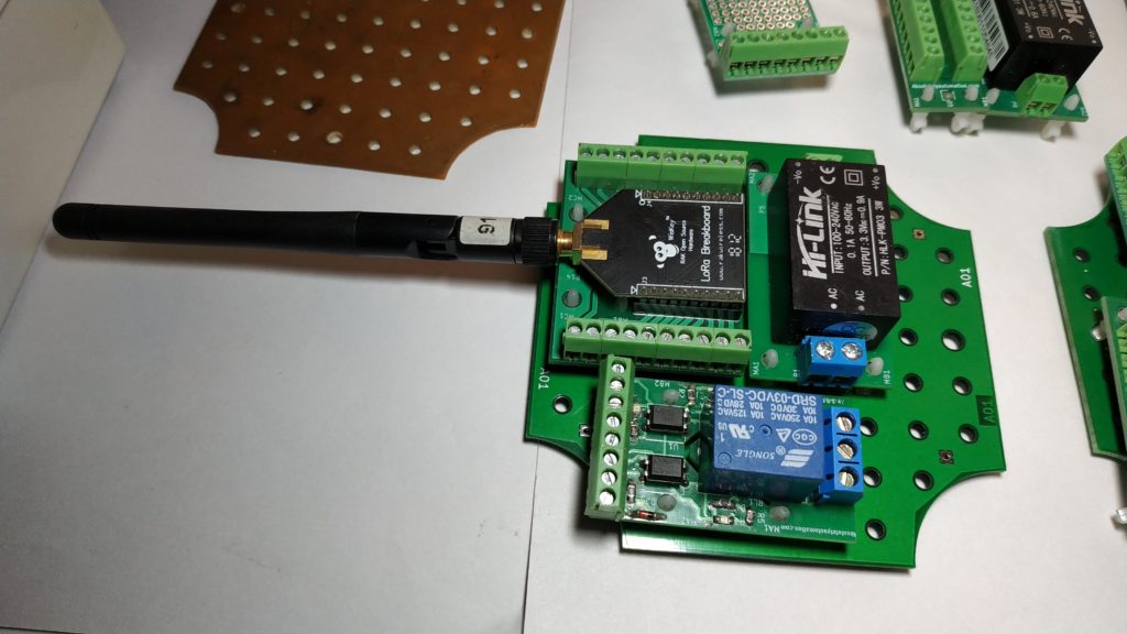
Device mounting.
Video: Full explanation
Conclusions
Initially Thanks to JLCPCB.com for allowing me to manufacture the motherboards, this system consists of many PCB parts, allowing dynamism and flexibility in assembling IoT projects.
Currently everything is being documented about the system, including gerber files to make them available to the public, formally even the system does not have an official name, for now it will be called the “sistemita”.
Thank you for being here, greetings from PDAControl, subscribe to our YouTube site and channel for more projects.
