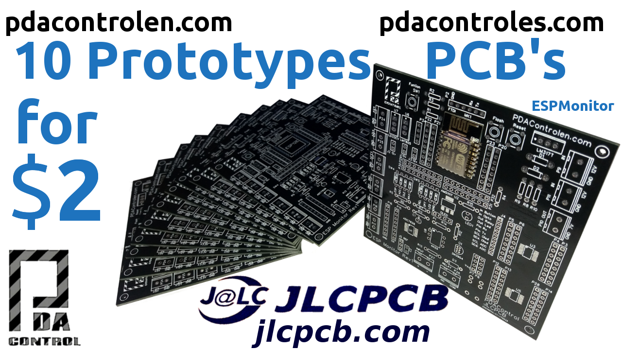
For a long time we have made our tests in protoboard, I think we already have a lot of tests that deserve a prototype for more robust applications, decided to take up the electronic design and I have found JLCPCB to provide a PCB manufacturing service at a price that very reasonable.
Based on some applications with esp8266, I designed the ESPMonitor Rev1 to facilitate long-term tests and assemblies, since I do not have the time, skills and quality. I have decided to do my design and send it to JLCPCB to manufacture my pcb.
In this case I will not show you how to make a prototype … we will make 10 for 2 dollars !!! in 3 steps.
A little more about JLCPCB
JLCPCB (Shenzhen JIALICHUANG Electronic Technology Development Co., Ltd.), is the largest PCB prototype company in China and a high-tech manufacturer specializing in rapid PCB prototypes and PCB production of small batches, excellent for our projects.

With more than 10 years of experience in PCB manufacturing, JLCPCB has more than 200,000 customers in China and abroad, with more than 8,000 online orders of PCB prototypes and small quantity PCB production per day. The annual production capacity is 200,000 sq.m. for several 1-layer, 2-layer or multilayer PCBs. JLC is a professional PCB manufacturer that has large-scale equipment, well equipment, strict management and superior quality.
How to make 10 prototypes at once
Only in 3 Steps:
1. The design
At some point we have created a schematic diagram in some of the available software Altium, Eagle, KiCAD, Ares(Proteus), Diptrace, PCBWizard, OrCAD(PSpice) among others, we can use any of the above, the only requirement is that they generate the Gerber file for manufacturing.
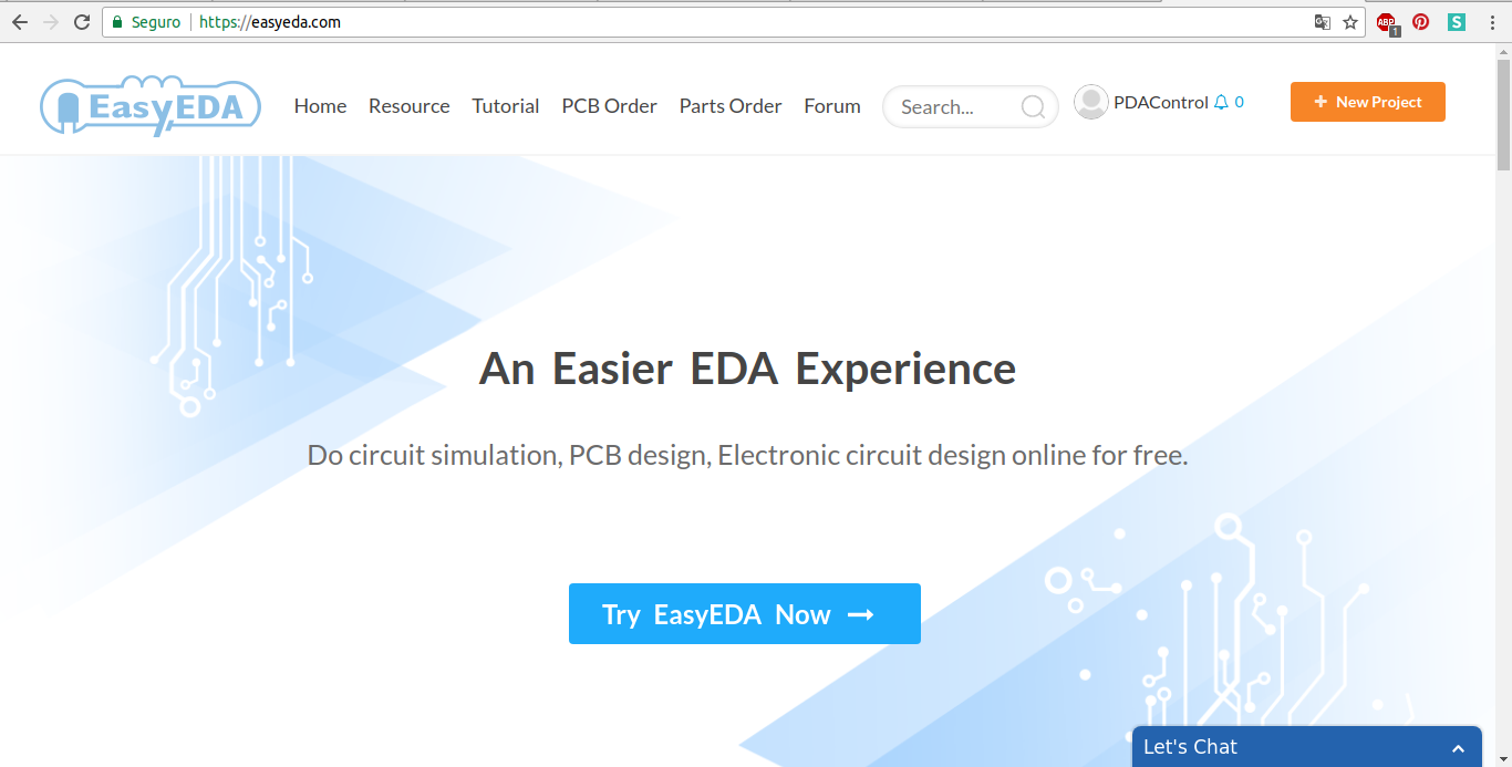
I have tried some of the software mentioned above, they are open source, others under educational licenses and others under commercial license, but in this opportunity I have tried, designing in EasyEDA.com is online design.
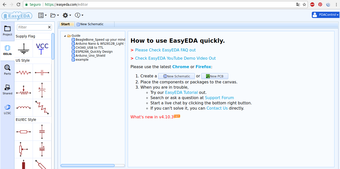
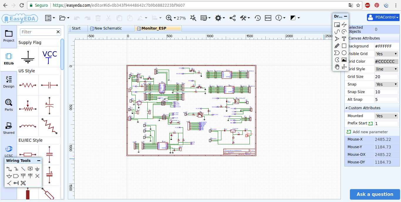
Finished Schematic Diagram
- Passive components
- SMD components
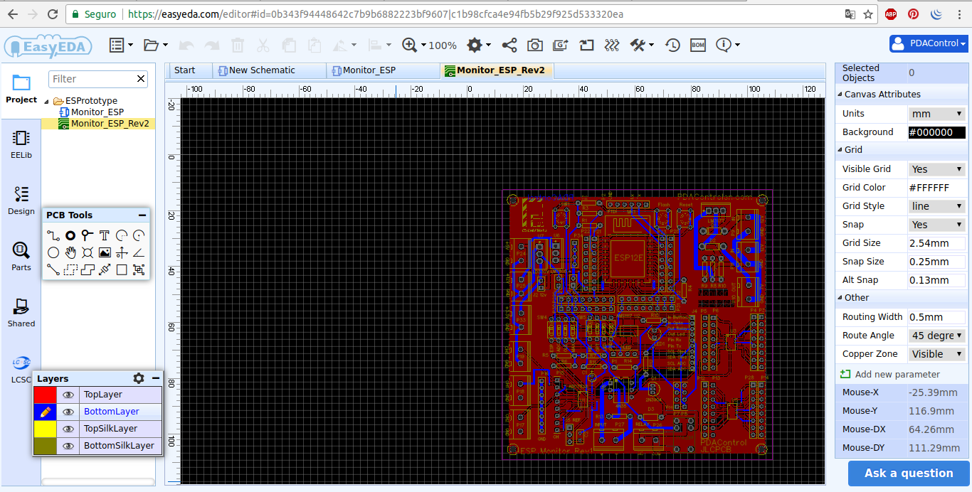
Finished PCB
- 2 layers.
- 100mm * 100mm
- mix between Auto routed and manual routing.
2. Generate GERBER File
Gerber is a file format that contains the information necessary for the manufacture of the printed circuit board or PCB. The most common standard today is the RS-274X, 1 although there are other less frequent ones.
Source Wikipeda : Gerber.
All the design software mentioned above allow generating this file, there are guides in the network to generate them without problems, in this case I will generate the Gerber file from EasyEDA.
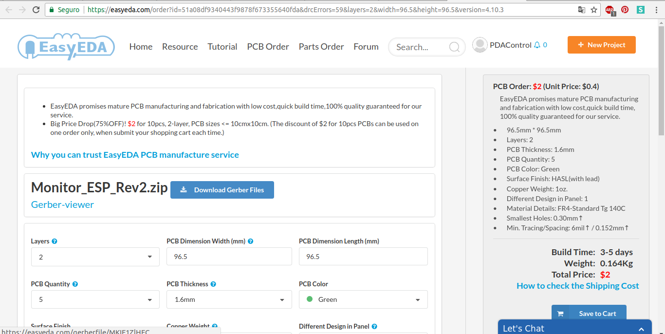
All the files must be saved in a compressed .zip in my case Monitor_ESP_Rev2.zip.
3. Create order and manufacture of pcb JLCPCB
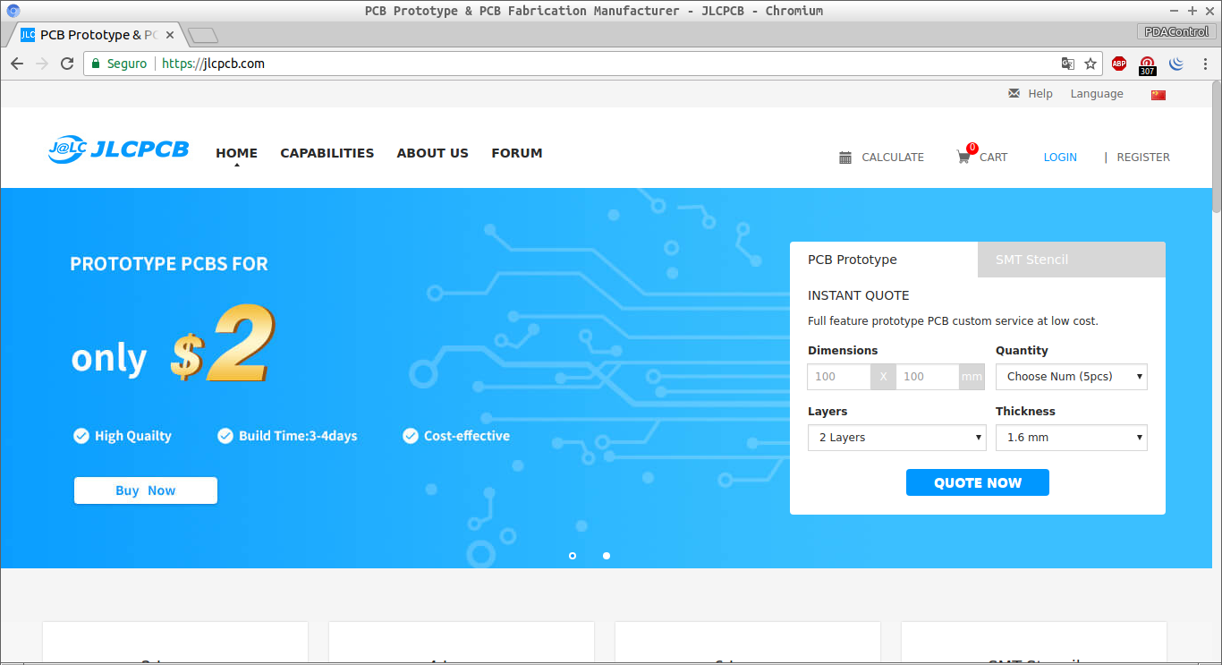
Login to https://jlcpcb.com
Register, fortunately if you design in EasyEDA the same account works in JLCPCB.

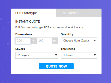
Enter initial design parameters:
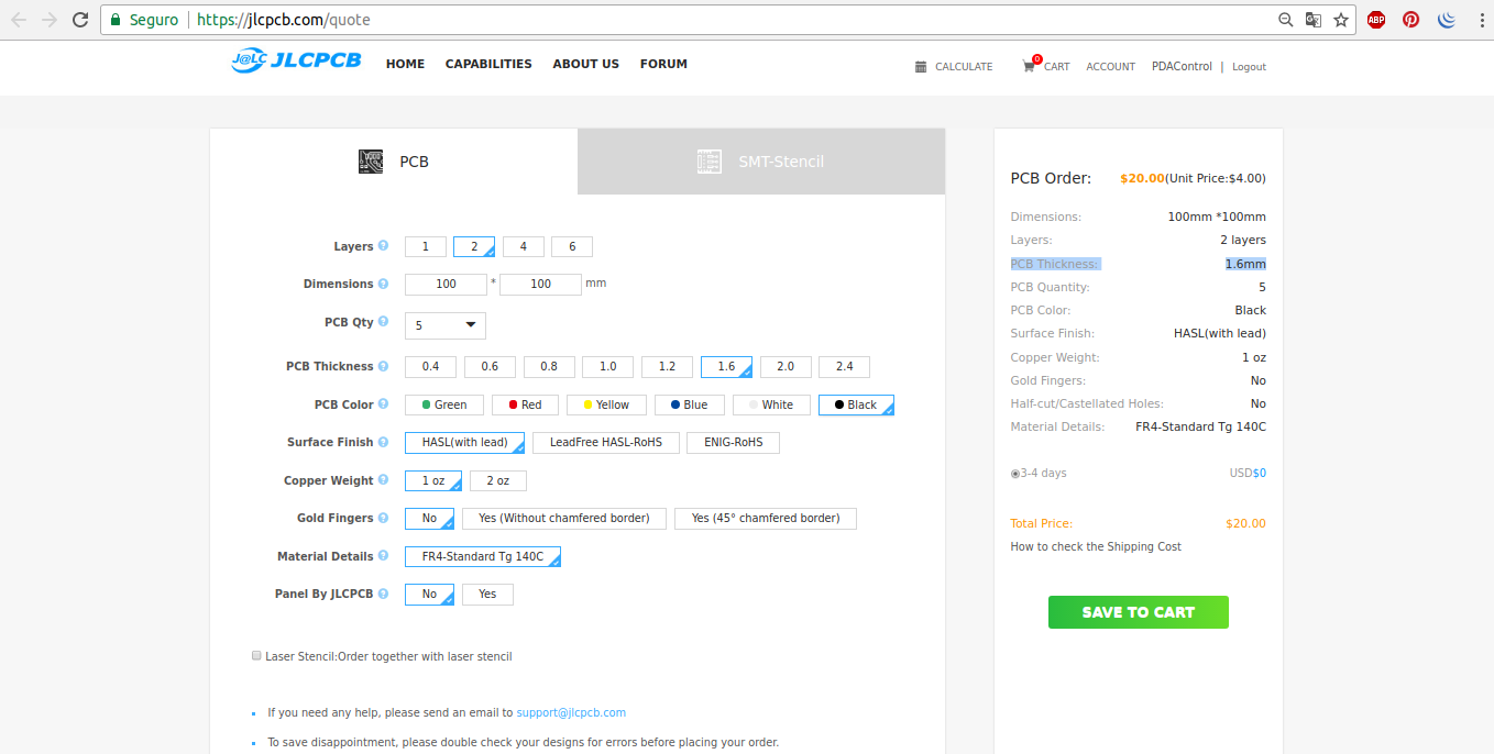
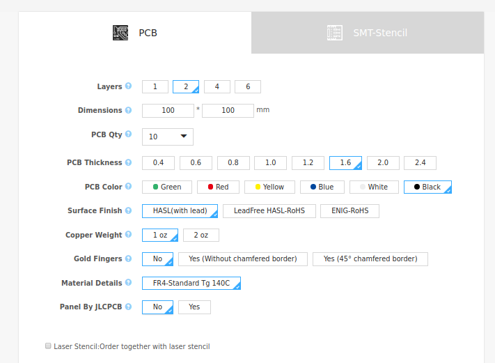
Characteristics of the PCBs in my case:
- Layers: 2
- Dimensions: 100mm x 100mm or smaller.
- PCB Thickness : 1.6, to make it strong.
- Color: Black, gives them character.
- Finishing of PCBs: HASL, finished in a weld bath that covers copper and prevents oxidation, facilitates welding.
- Copper Weight : 1 Oz.
- Gold fingers: I do not need them, they are connectors on the edge of the PCB similar to a slot.
- Manufacturing Materials: Standard-FR4, corresponds to a standard for the manufacture of safe materials.
- Panel by JLCPCB: Not necessary, My pcb is 100mm * 100mm occupies all space, This option allows to replicate small pcb’s in a large panel, I create detailed information Panel by JLCPCB
I do not require any special or additional features on my pcb.
Add to cart.
Add file GERBER
Upload Gerber file compressed to JLCPCB:
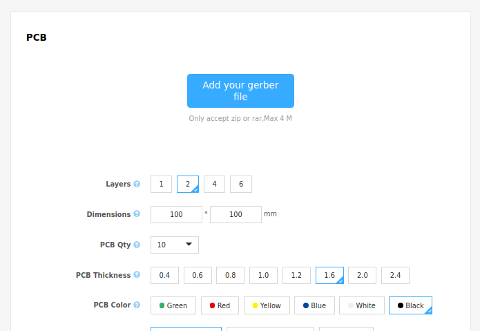
File successfully uploaded:
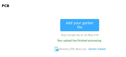
Let’s visualize how the PCB will end up using Gerber Viewer:
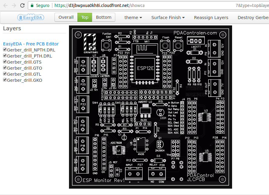
After uploading the Gerber File, the actual dimensions of the PCB will be displayed in my case:

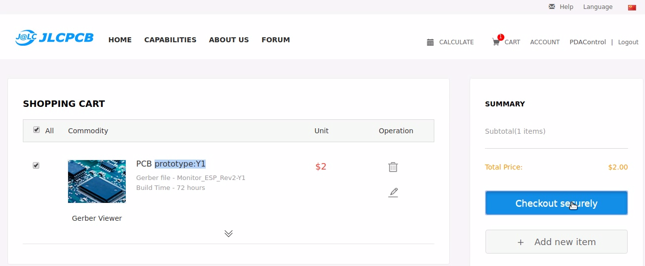
Add, display Car and press “checkout securely” :
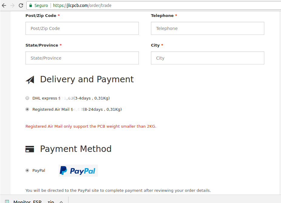
Delivery and Payment
Fill the form complete with data.
Select method of delivery, has 2 modes from DHL very fast, and Registered Air Mail takes its time but it arrives perfectly, everything depends on the personal urgency for the PCBs and therefore reflected in the cost of the shipment, I have used both services and perfect !!
Select payment method, allow Credit Cards and Paypal.
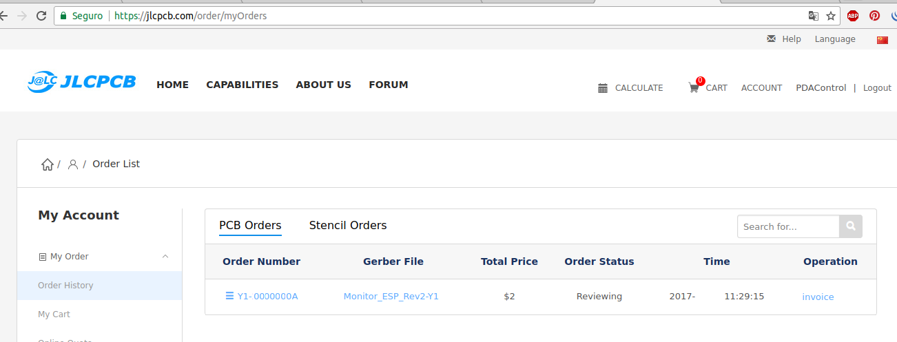
Finally “PAY” and at the end will visualize an order similar to this and wait for my pcb’s.
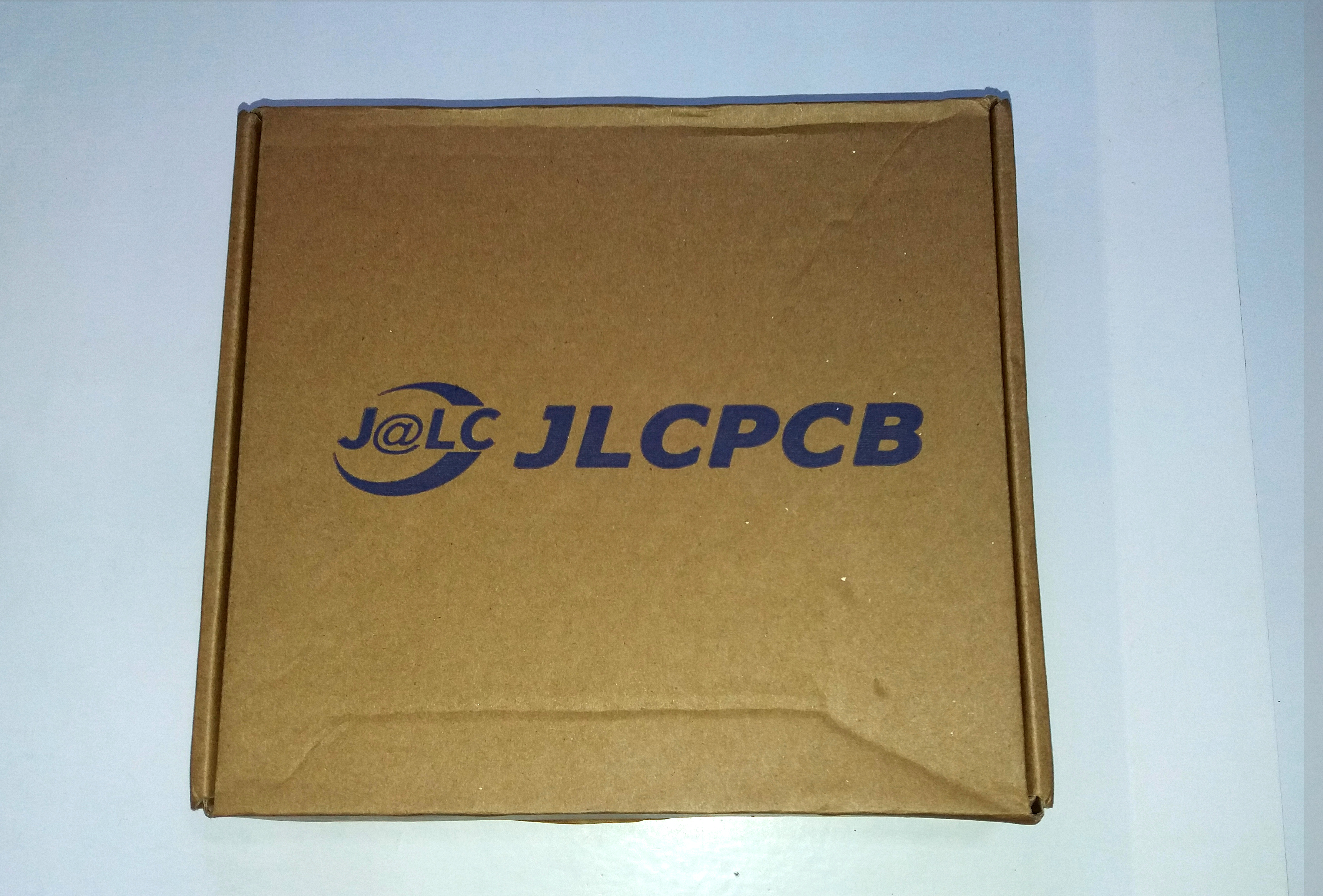
The PCBs arrived
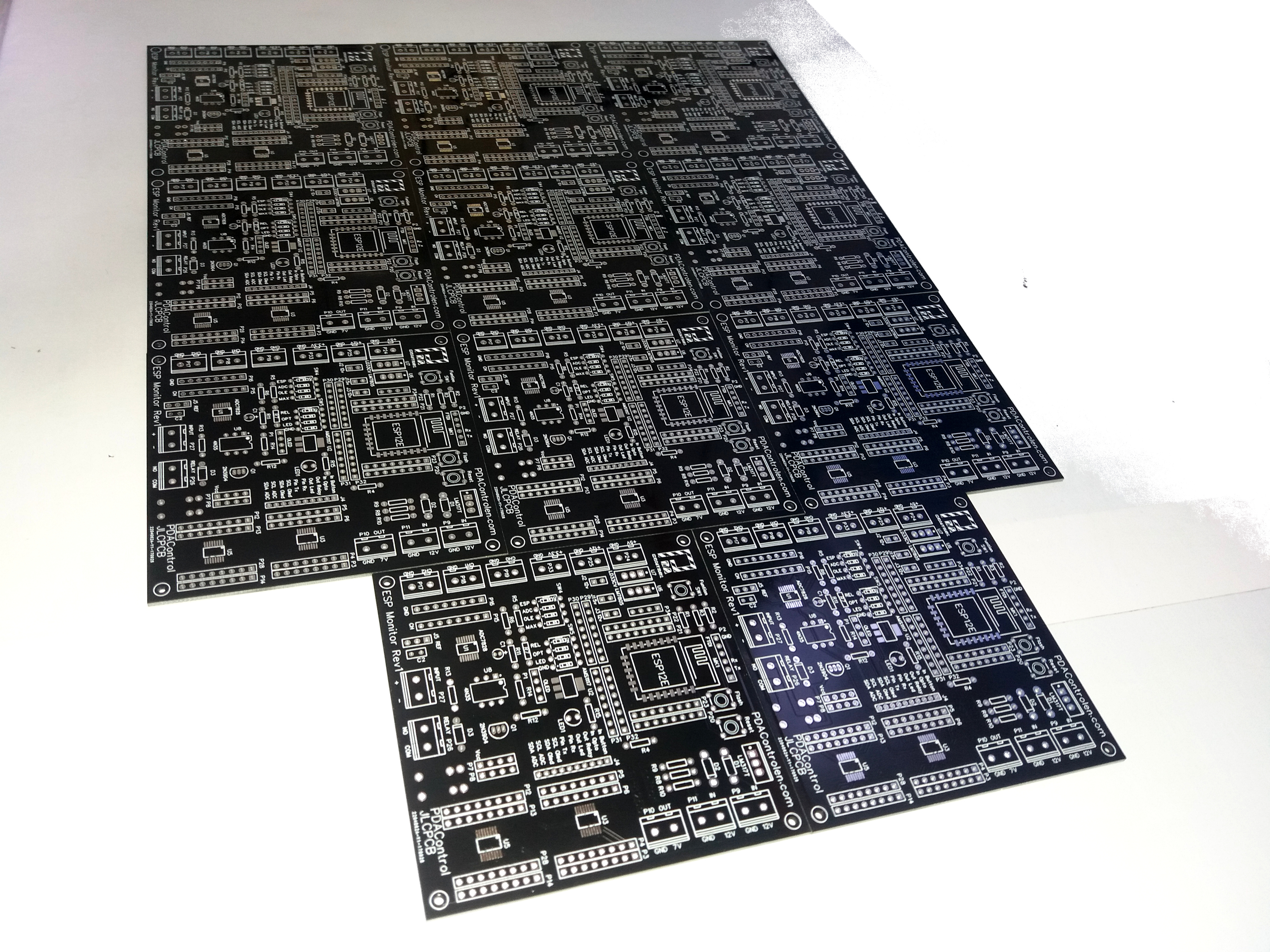
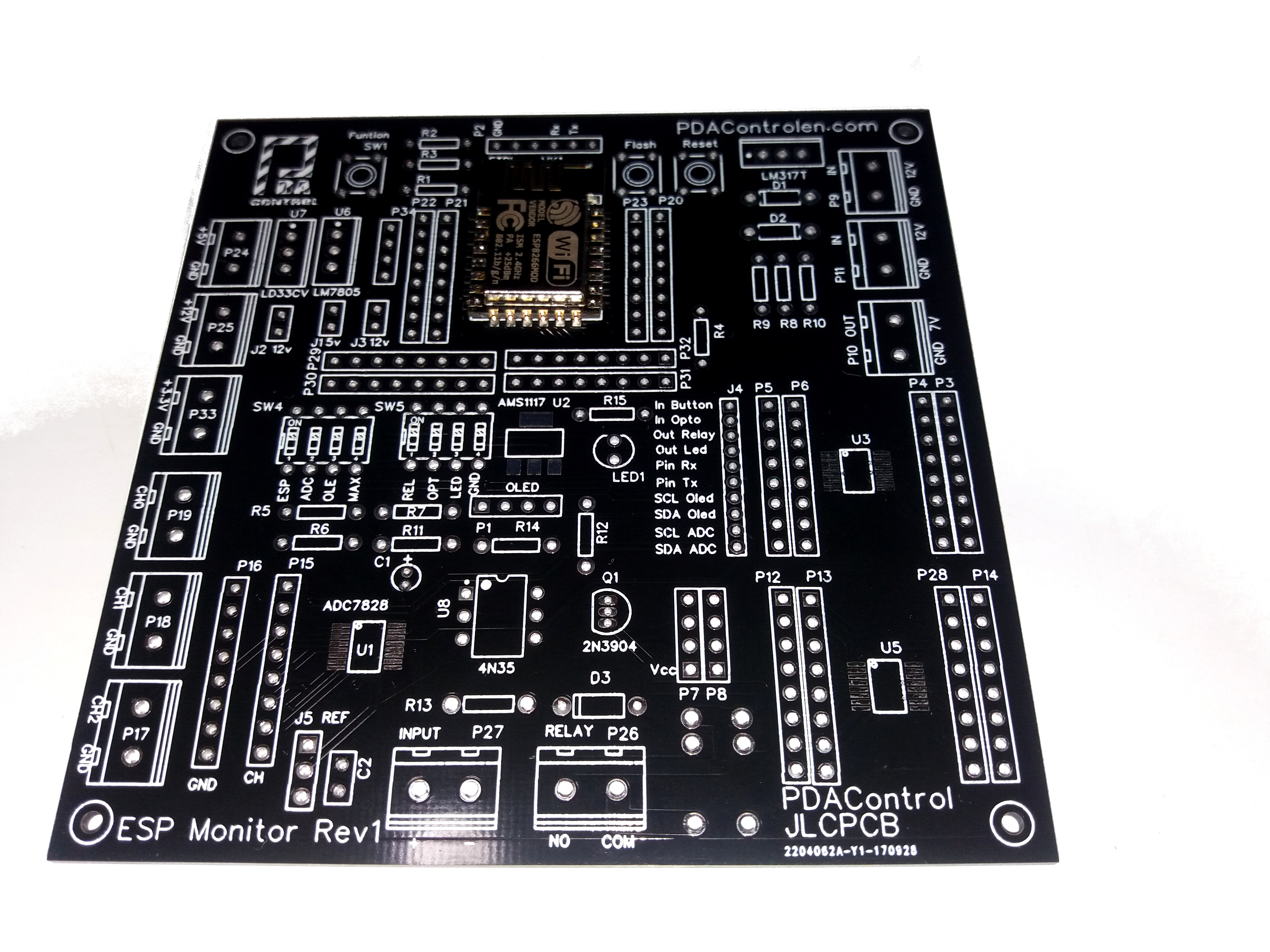
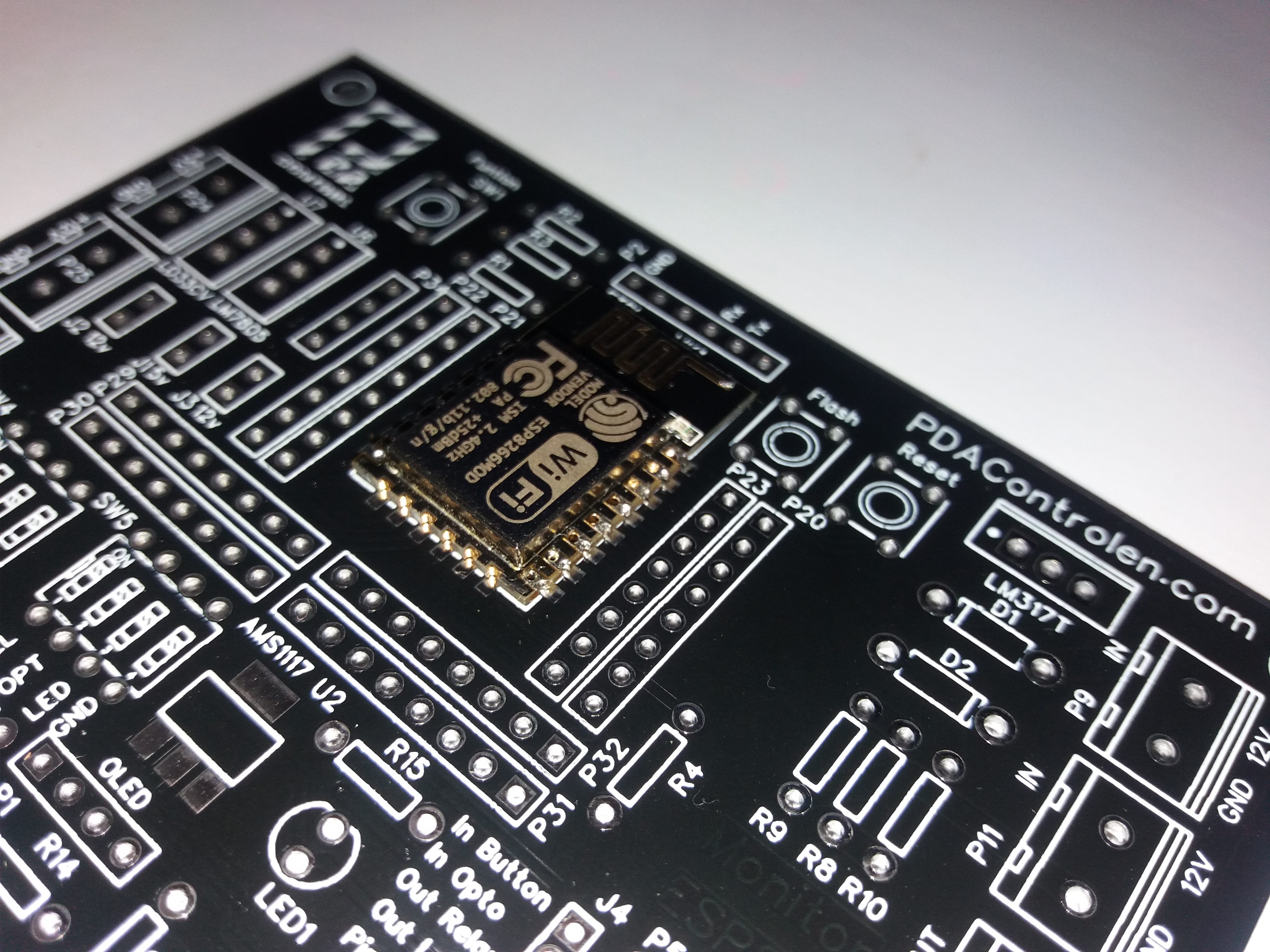
Some images of the PCB’s of my prototype ESPMonitor Rev1 wooow !!!! I’m anxious to weld.
The PCBs were excellent, the quality robust, strong and very beautiful.
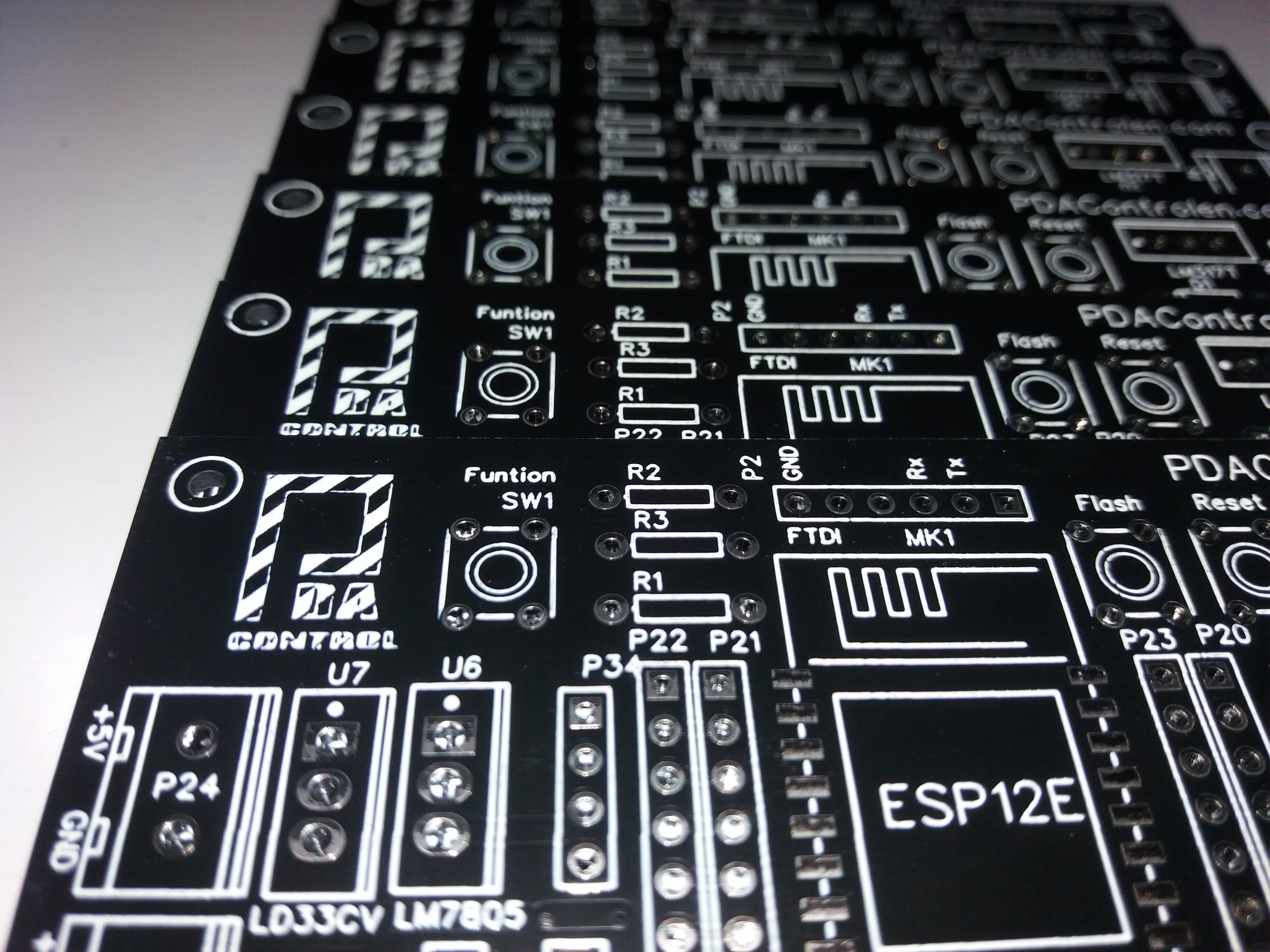
To prove the quality, I added details and the screen printing replied without problems.
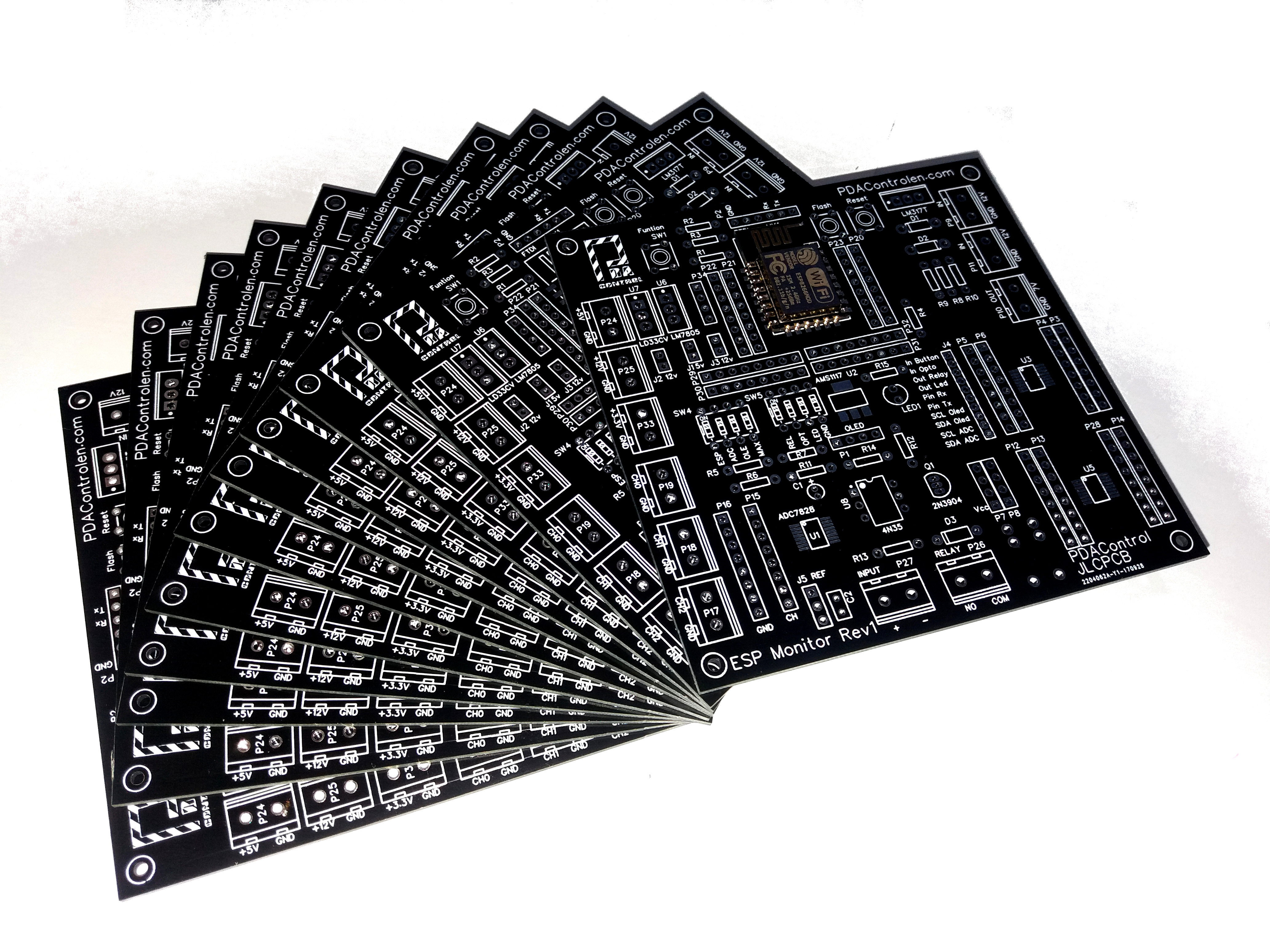
10 for 2 dollars!
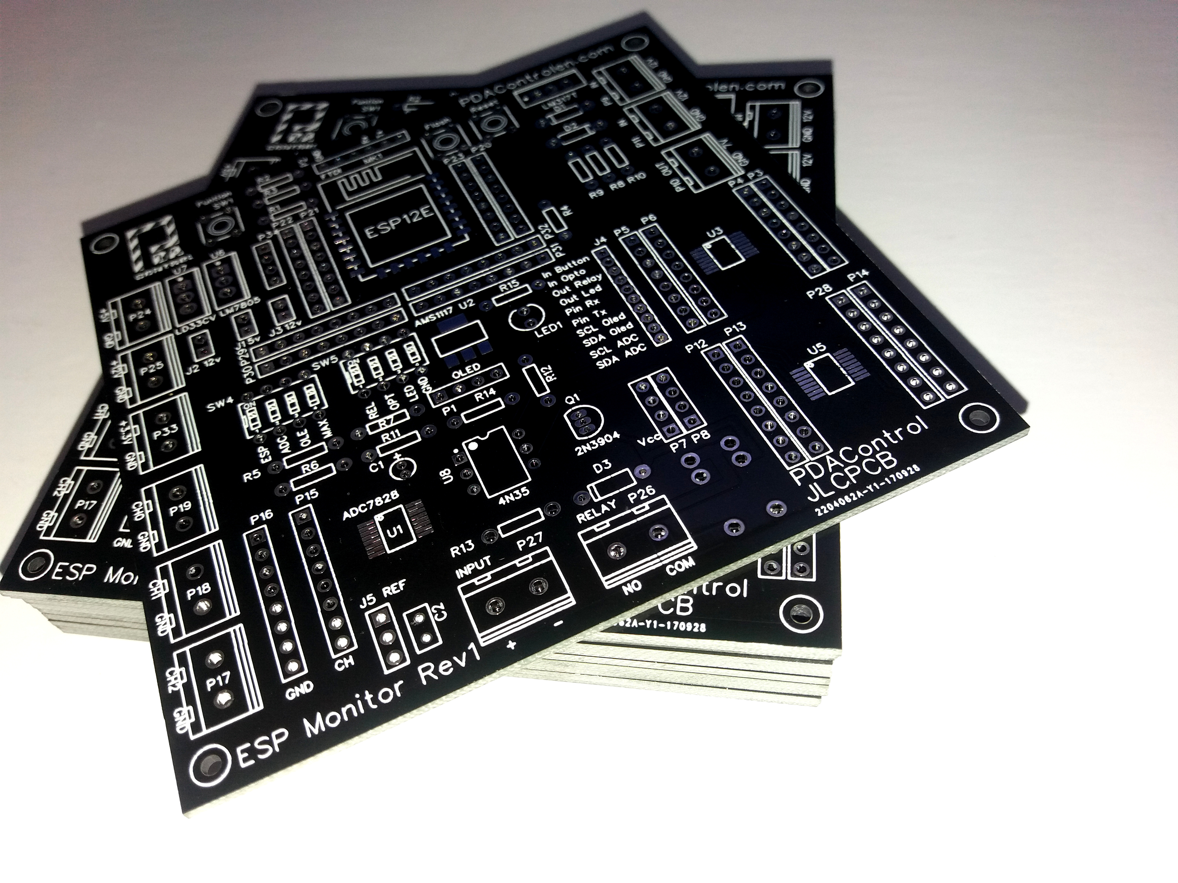
The quality of the Logo !!!!
Complete Tutorial : 10 Prototypes PCB’s por $ 2 ESPMonitor Rev1
Conclusions
This is a very good option in this case with ESP8266 12E, a long time ago I do not make a homemade pcb from scratch, personally I would spend a lot of time and effort.
I prefer this option with JLCPCB because professional PCB’s are created at very low cost 10 PCB’s at 2 dollars, each pcb at 0.20 dollars … I could never manually do it for that price.
Allow to select the finish, the incredible black color, the quality of the PCB’s and the impeccable serigraphy.
I’m really happy, in a very short time I made a prototype according to my own requirements and functionality, to weld the ESPMonitor Rev1.
I recommend this service as they mention on their page jlcpcb.com.
- Very good price.
- 100% guaranteed quality or rebirth.
- Good delivery time: 3 days by DHL.
- Online purchase order.
- Technical support, in case someone responds.
Regarding the design, you can use any platform that allows you to generate the gerber file, maybe in the next tutorials you will do it from KiCAD, Eagle will use it some years ago but for now I will try to use Open source.
