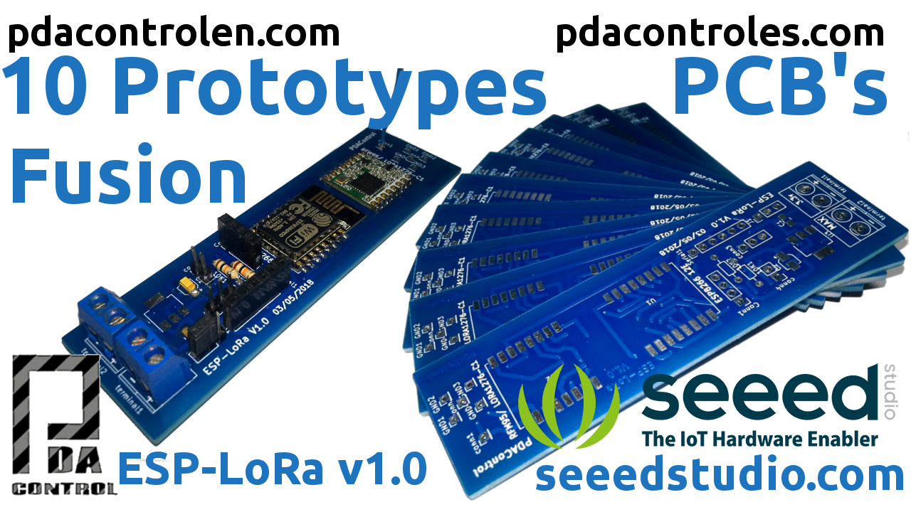
A few days ago I finished tests on my breadboard, being positive I decided to migrate my project to a pcb not only for functionality and practicality, but also for aesthetics, I have chosen the PCB manufacturer company Seeedstudio.com, we all know it as a manufacturer of hardware and IoT solutions , but they also have a PCB manufacturing service. I want to prove how my new ESP-LoRa / LoRaWAN prototype is. And making 10 prototypes is very simple and very economical for $5 USD.
Recommeded: Getting started, considerations and concepts LoRaWAN # 1
Let’s learn more about Seeedstudio
All at some time we have seen their wide variety of sensors, hardware, modules and their store, seeedstudio apart from being a manufacturer and distributor of IoT hardware, if you are a hardware manufacturer they would provide accompaniment as an ally in the integration of your project With IoT Platforms, its headquarters are located in Shenzhen, China and also has branches in the United States and Japan, they can easily distribute worldwide.
more info: seeedstudio.com/about

In this case we will not talk about your hardware platforms, we will use one of your services, our PCB Fabrication case for only $ 5 USD !!!! in Seeedstudio. also has other services that we will see later.
Other Services Available
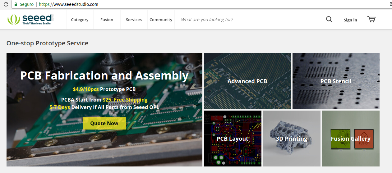
Fusion Advanced PCB
This service allows us to manufacture our PCBs with many more specifications. Its main features are:
- More material options for pcb.
- Personalized stacking
- Better capacity in the manufacturing process.
- Mass production process.
- More info: Advanced PCB.
PCB Stencil
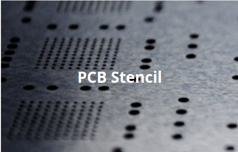
fabrication service “Stencil” is a template used to apply solder paste to the pad where SMD surface mount components will be placed.
- More info: PCB Stencil.
3D Printing
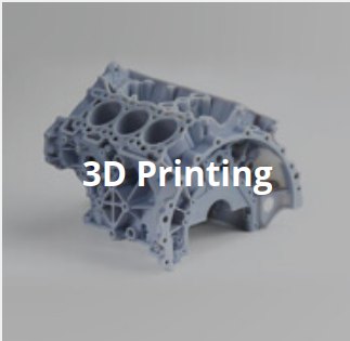
Seeed Studio has a 3D printing service, requires our .STL file, and certain manufacturing parameters are determined, I recommend to contact Seeedstudio. engineers beforehand.
More info: 3D print.
PCB Layout
They also have a complete PCB design service, basically it is upload schematic EDA design file or a schematic PDF and component listing file and configure other parameters, I recommend to contact Seeedstudio. engineers beforehand.
More info: PCB Layout.
Fusion Gallery
Seeed Studio has a community or space to share our designs and download other designs, there are several categories available.
More info: Fusion Gallery.
PCBA Seeed Fusión – PCB Assembly Service

This is the service that has caught my attention“Seeed Fusion One-Stop prototipo PCBA”, this service of manufacturing and complete assembly, small lots of prototypes of high quality, affordable and reasonable prices, is perfect for engineering companies, manufacturers , Kickstarter projects and students, Perfect in case you want to make 100 prototypes will arrive ready to just connect and work, Manufacturing in 3 steps:
- Load gerber file “Design of our PCB”.
- Load BOM format “Components”
- Instantly a full quote will be generated.
Scope of Prototype Testing
Seeedstudio has the required tests for the prototype from gpio’s voltage I2C / Uart/SPI/CAN/Onewire SWD Temperature / Humidity / Atmospheric Pressure / Luminance to communications such as GSM/WCDMA/LTE GNSS Bluetooth/LE Ethernet NFC 802.11/b/g/n/a/ac among others, they are also in the capacity to generate certifications in their laboratories.
More info: Seeed Fusion One-Stop prototipo PCBA / PCB Assembly Service.
How to make 10 Prototypes at a time
1. The Design
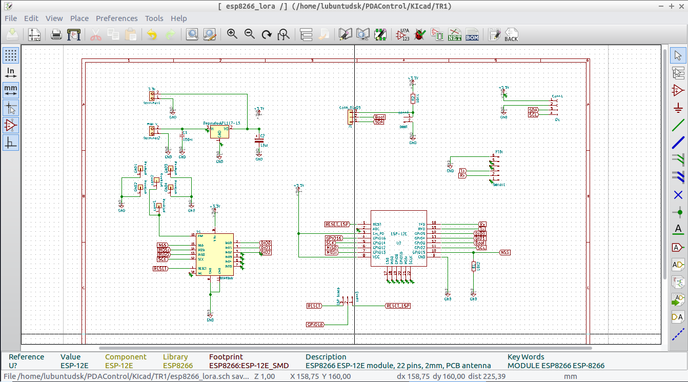
I have decided on this occasion to use KICAD to design my ESP-LoRa prototype, I have mentioned other well-known PCB design platforms before, but I have seen the advantages of Kicad since it is an Opensource software, there are no restrictions of use.

Recommended: Kicad installation.
Schematic Diagram
- Check “Electrical Rules check”.
- Export Netlist.
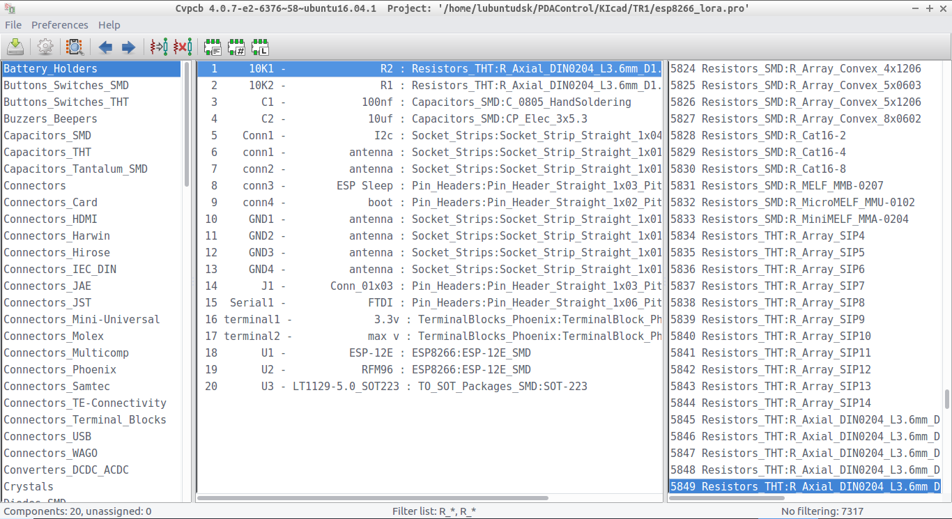
Assign components to their respective encapsulation
- Note: Check the sizes in the viewer correctly.
PCB design
- Import Netlist.
- Perform DRC checks.
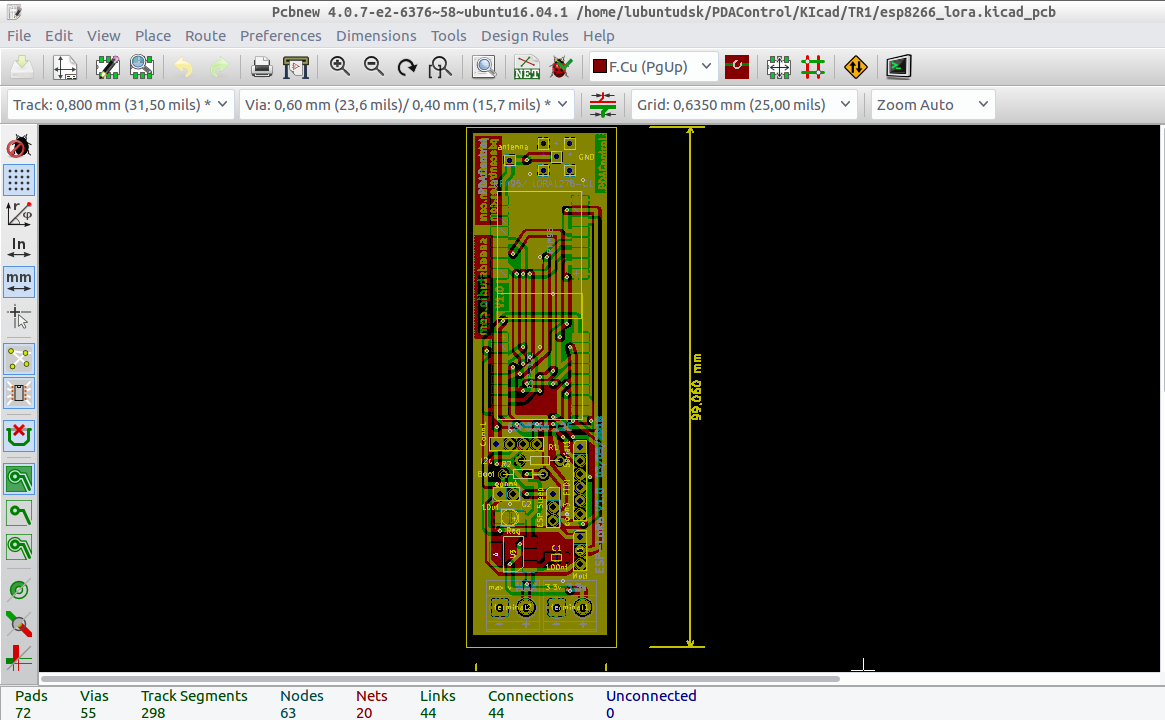
PCB Terminada
- 2 layers
- 95.2 x 22.2mm
- Manually Routing
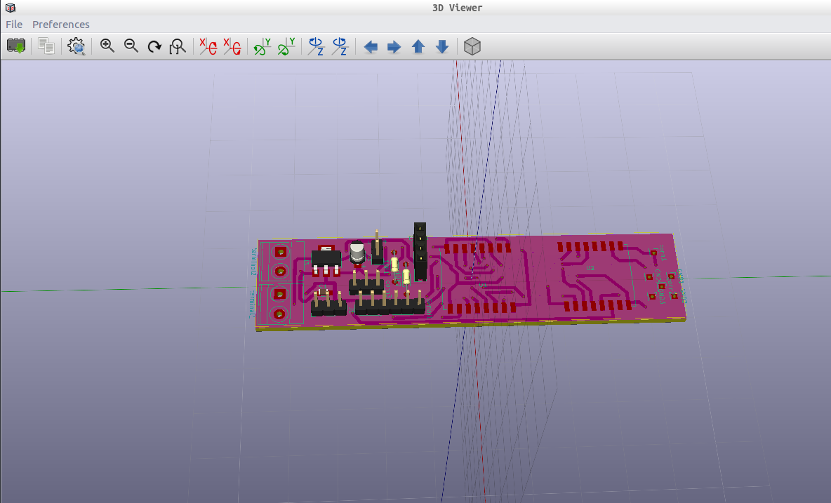
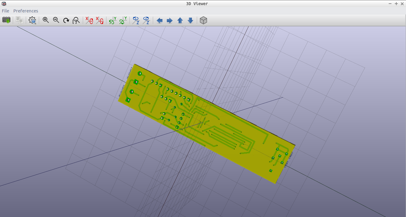
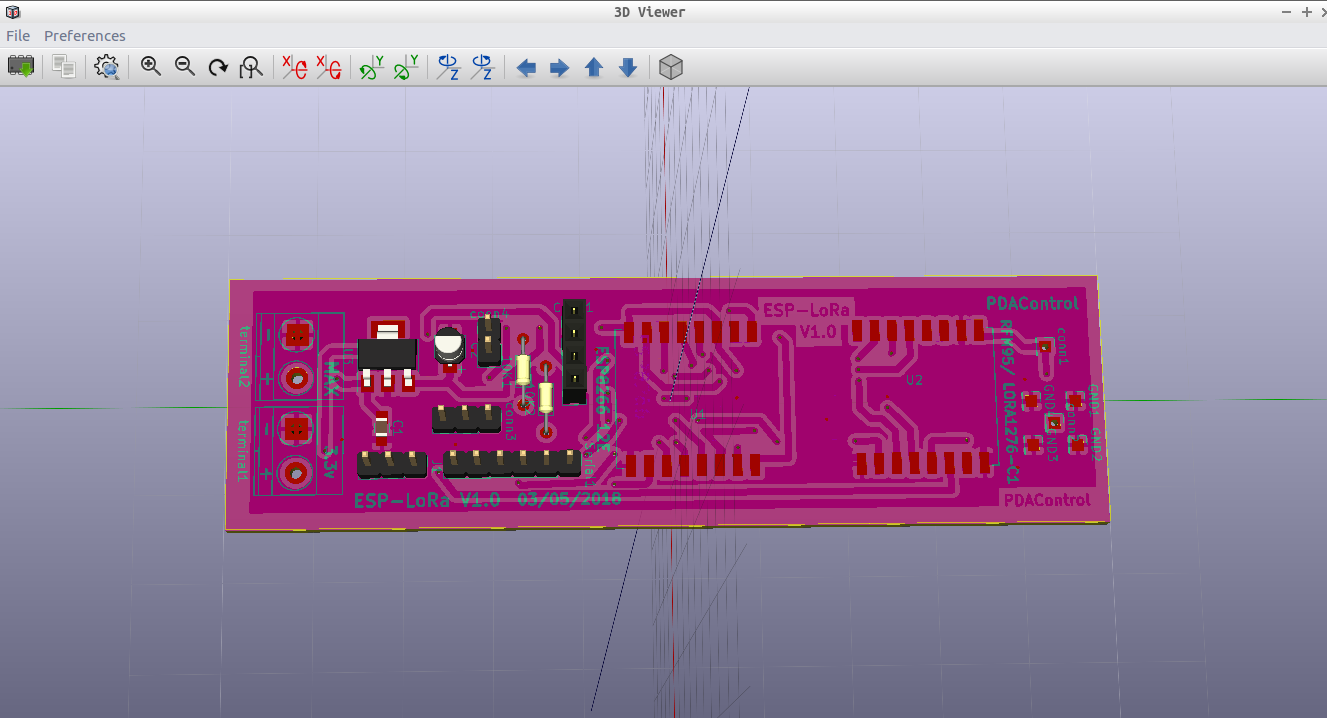
3D View KiCAD:
Viewer included in KiCAD that allows to preview the finish of our design
Generate Gerber File
Gerber is a file format that contains the information necessary for the manufacture of the printed circuit board or PCB. The most common standard today is the RS-274X, 1 although there are other less frequent ones.
Source Wikipeda: Gerber
All PCB design software allows to generate them:
Select PLOT and select the required ones, seeedstudio details in the following tutorial:
Recommneded: How to generate Gerber and drill files from KiCad.
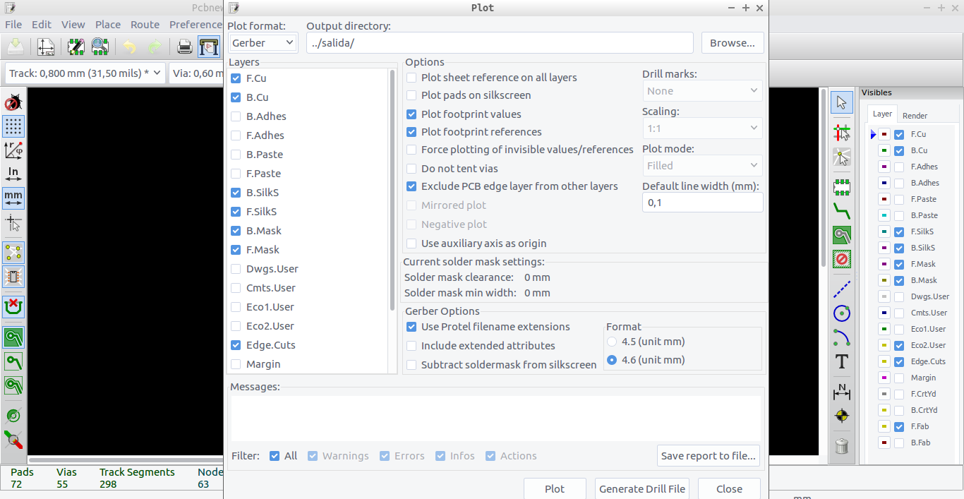
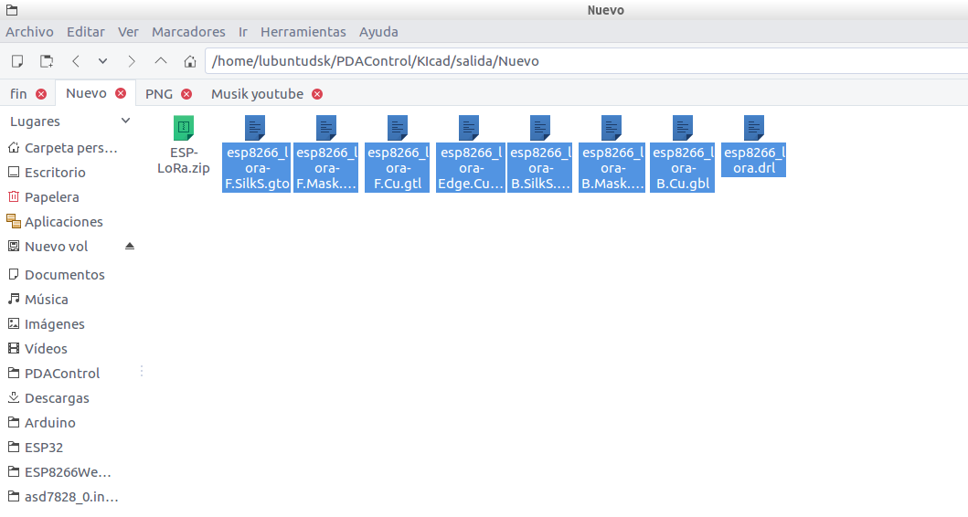
Generate a .zip compressed file, with the generated files, in my case these 8 files.
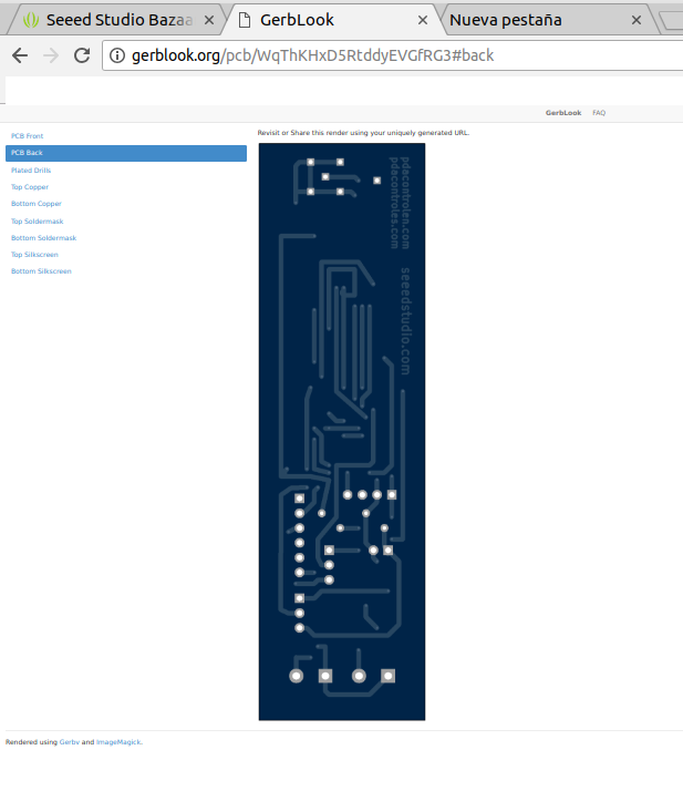
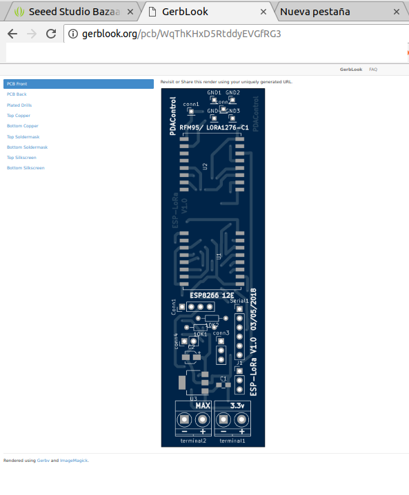
View Gerber Online file
In this opportunity I will visualize the gerber files, in the online viewer gerblook.org, we simply upload the compressed file.
3. Create order and manufacture of pcb Seeed Fusion
Login to seeedstudio https://www.seeedstudio.com/
Register or create account in Seeedstudio.
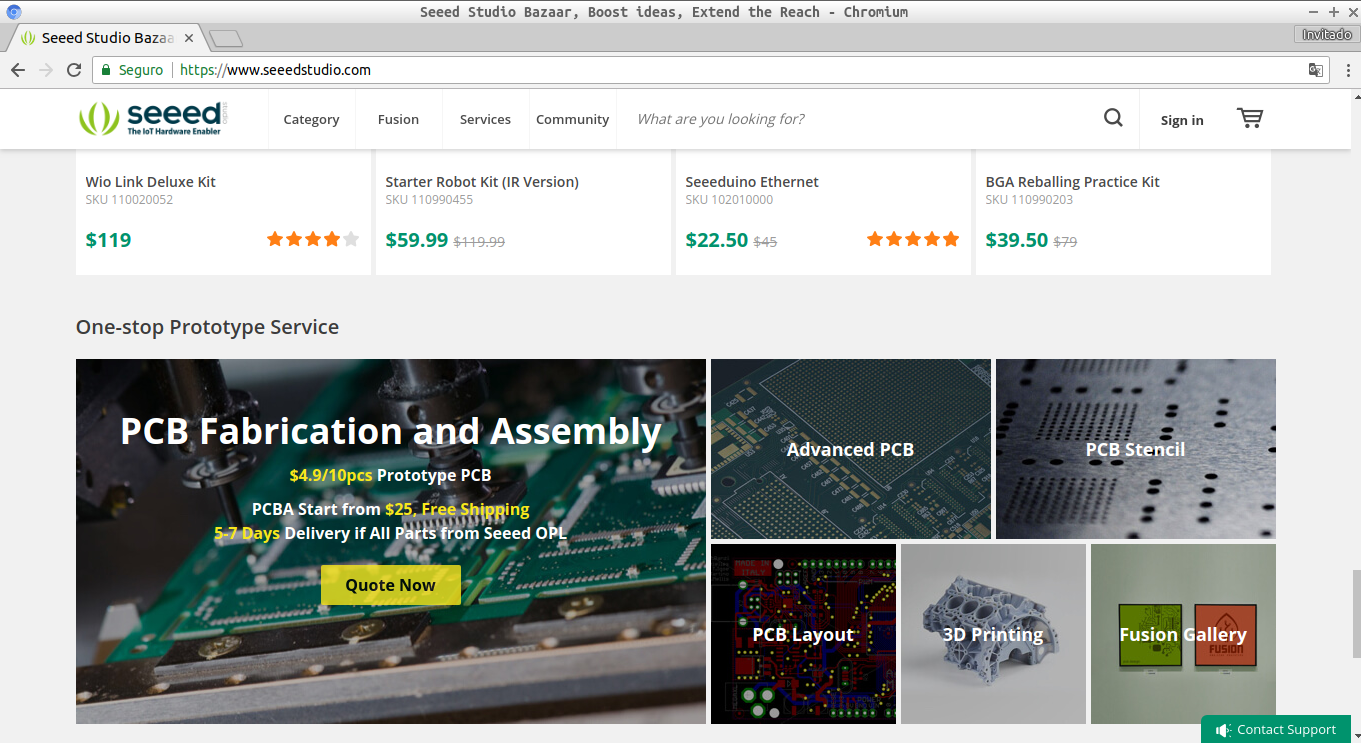
- Go to the end of the page “One-stop Prototype Service”
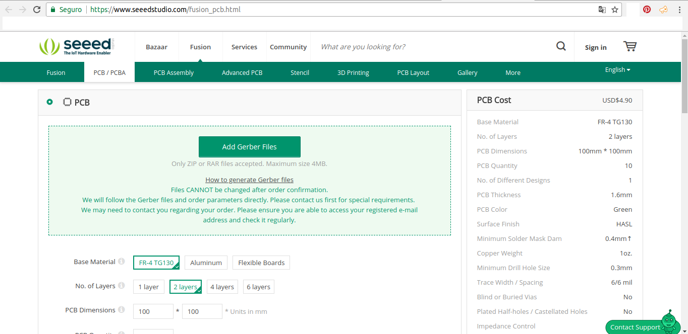
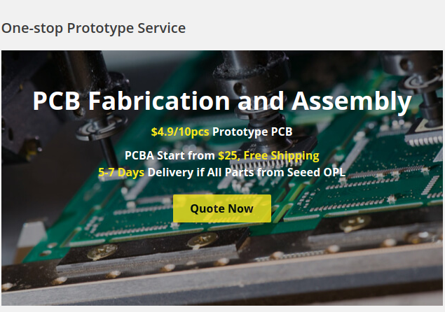
We enter Fusion PCB https://www.seeedstudio.com/fusion_pcb.html
Initially we added / uploaded our Gerber file “compressed”.zip.

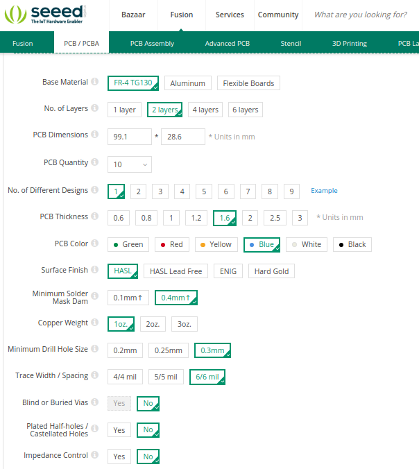
Enter initial design parameters:
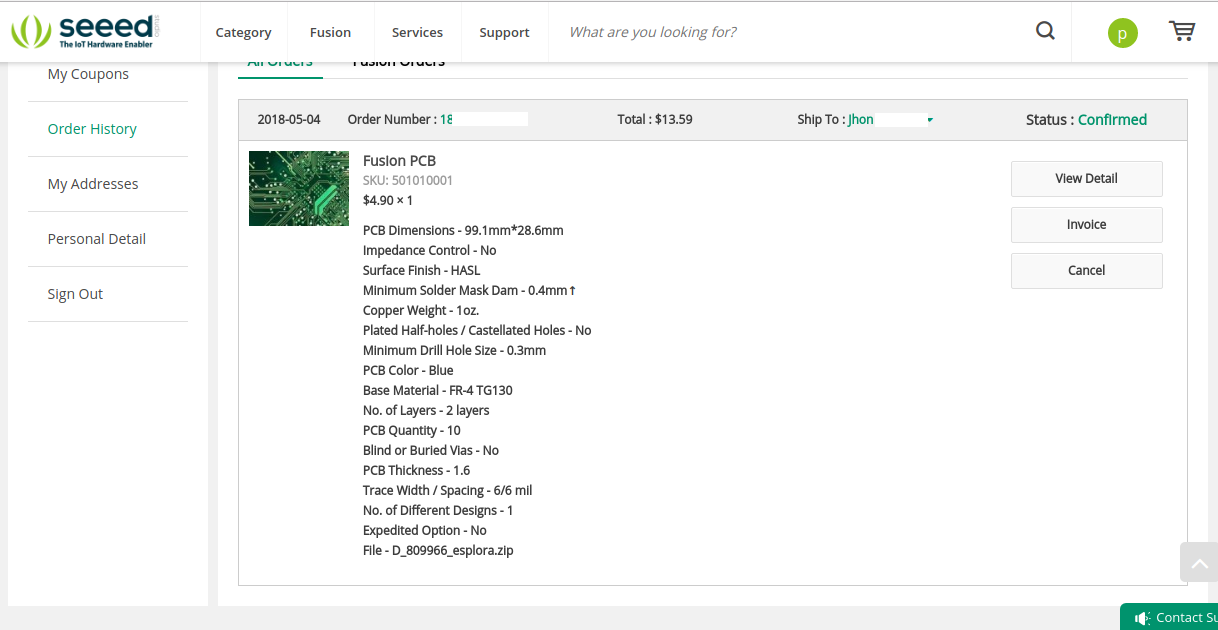
Characteristics of the PCBs in my case:
- Base material: FR-4 TG130, more information on FR-4
- Number of layers: 2 layers
- PCB Dimensions: 99.1mm x 28.6mm or more information about dimensions.
- Amount of PCB: 10 pcb’s
- Number of different designs: 1
- Thickness of PCB: 1.6mm
- PCB Color: Blue, A finish like the Arduino boards
- Surface finish: HASL
- Minimum welding mask dam: 0.4mm ↑
- Copper weight: 1 oz.
- Minimum size of drilling hole: 0.3mm
- Trace width / spacing: 6/6 thousand
- Blind or buried vias: No
- Silver half-holes / Hollow holes: No
- Impedance control: No
Add to Cart
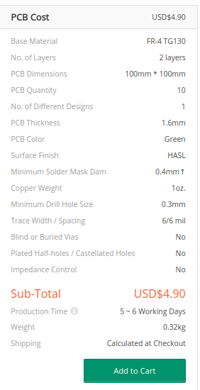
Added to Cart.
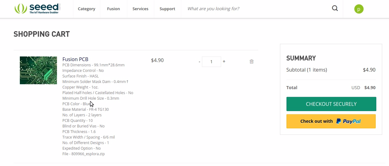
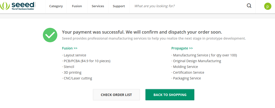
Make Payment CHECKOUT SECURELY or PAYPAL, enter CHECKOUT SECURELY, It’s $ 4.9 USD for pcb’s
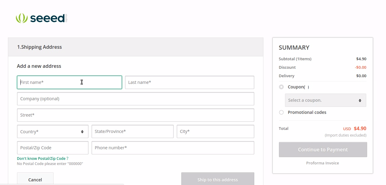
Shipping Address.
Fill out Form with information for sending receipt:
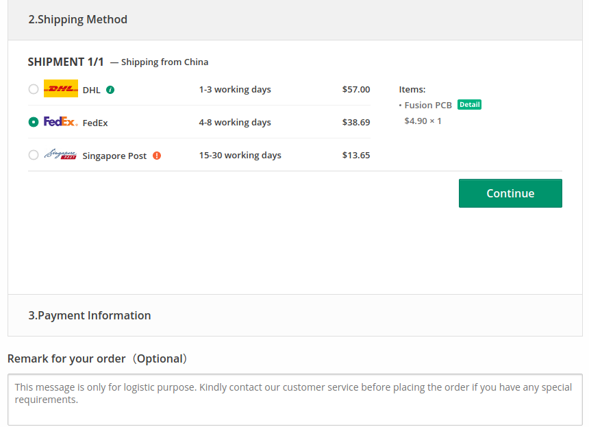
Shipping method
Shipping method, this time I will use FedEx, they can use the method they want, only the arrival time of the package varies.
Note: of course the value of the shipment varies by country.
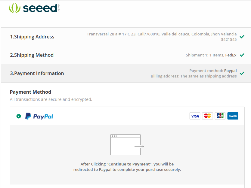
Payment method
It allows 2 methods of Payment PAYPAL and Credit Card, in my case I will use PAYPAL.
Payment Made and Dispatched Order.
Let’s check the State of Order
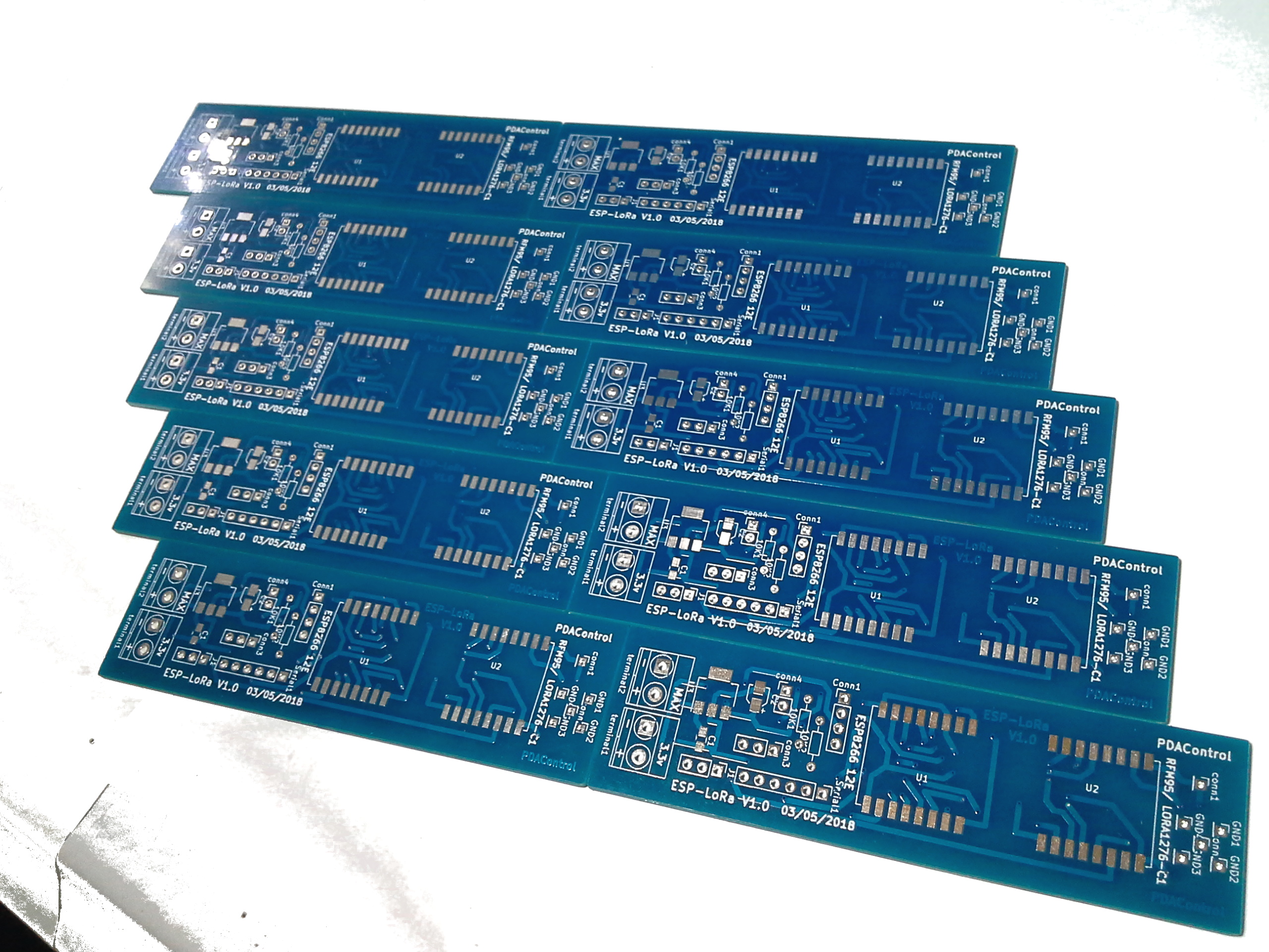
My new Pcb’s arrived !!!
Some days later, Approximately 7, via FedEx, my PCBs are the first version of my own LoRa nodes with ESP8266, we are going to see some pictures, and we will see in more detail the pcb.

The mask of components very well, although officially it is my first design in KiCAD.
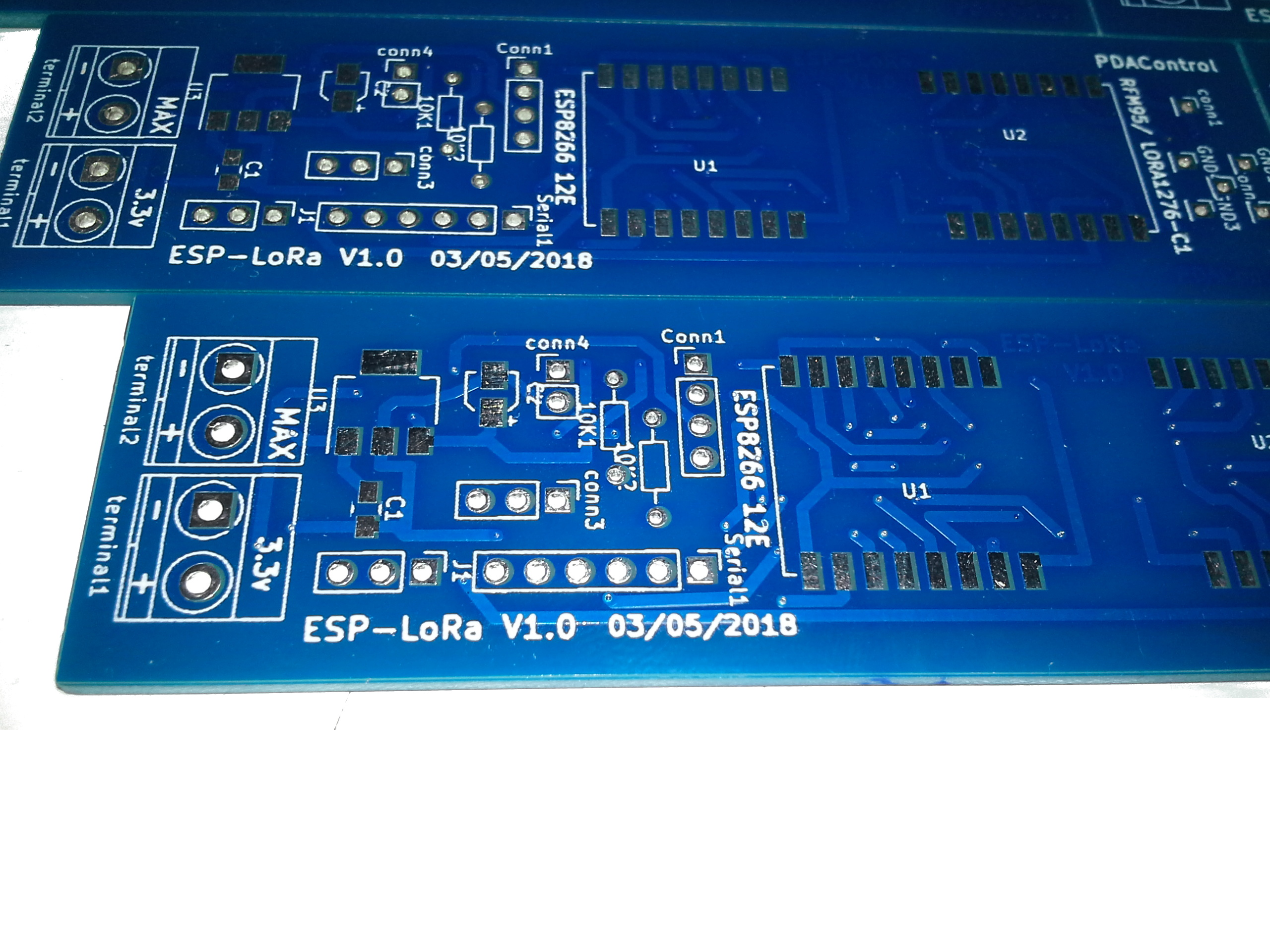
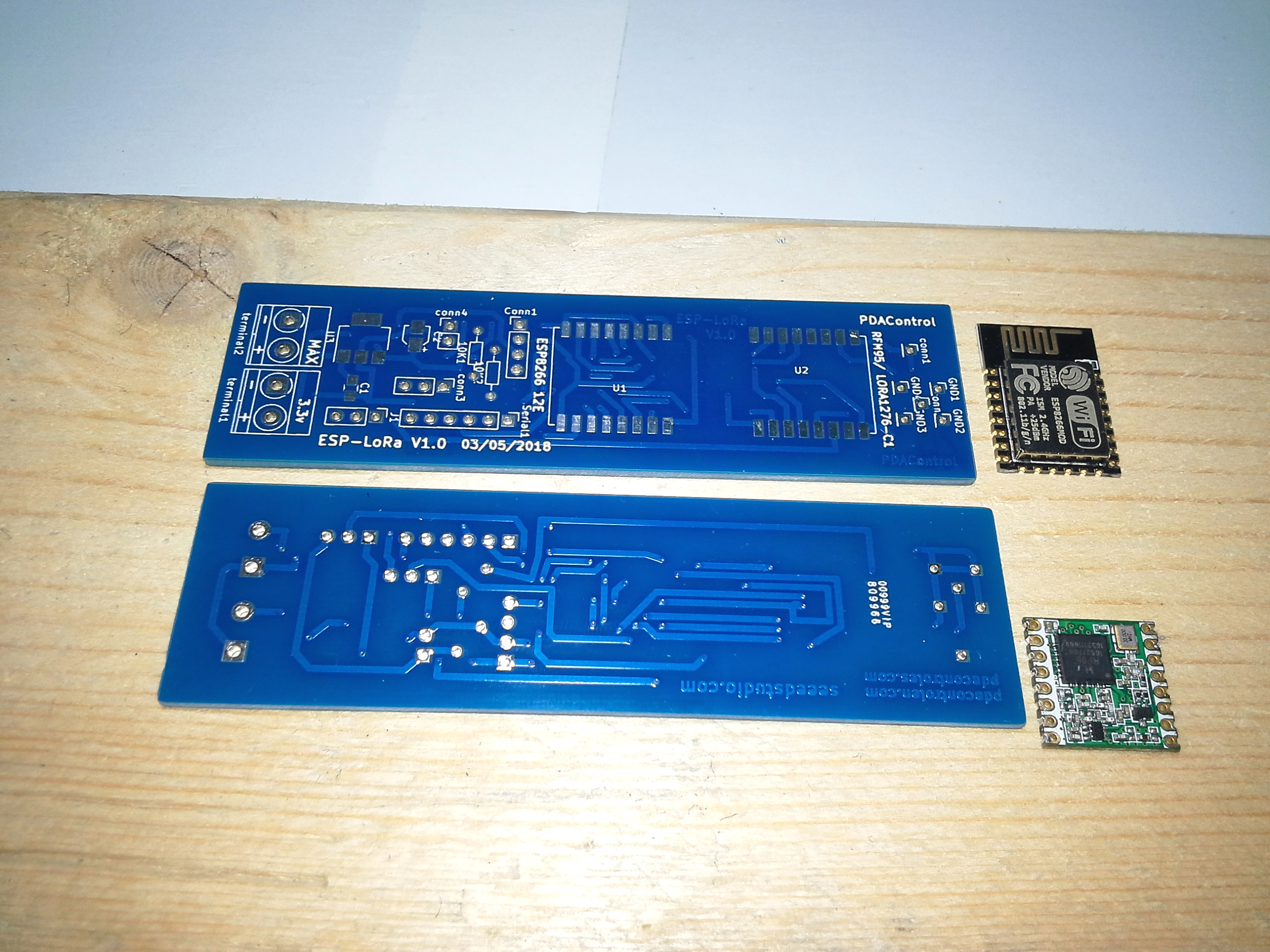
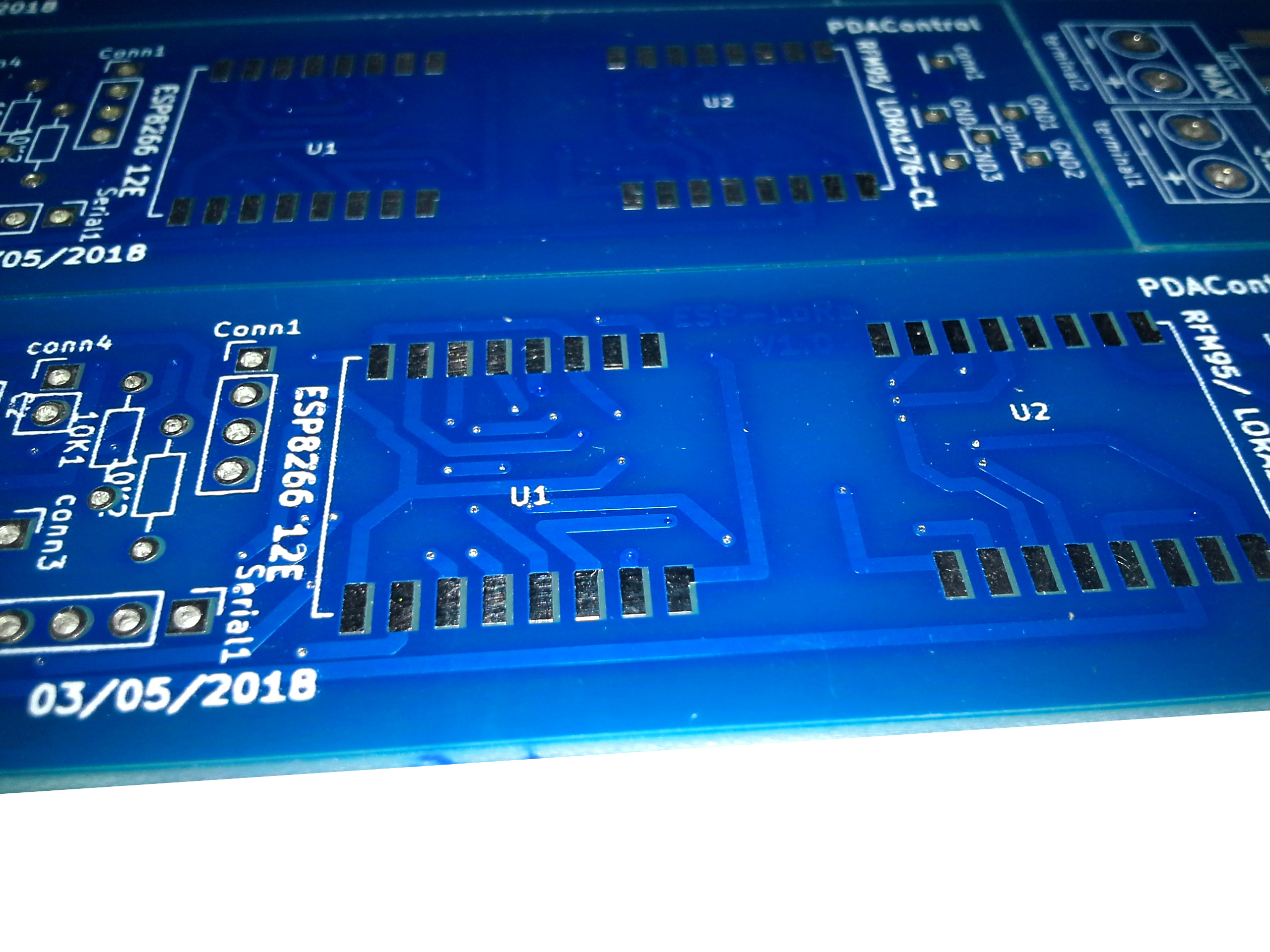
They were excellent!
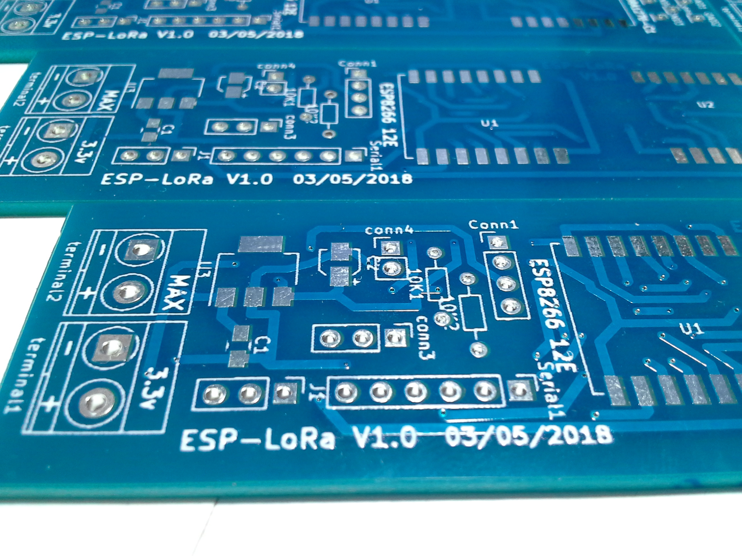
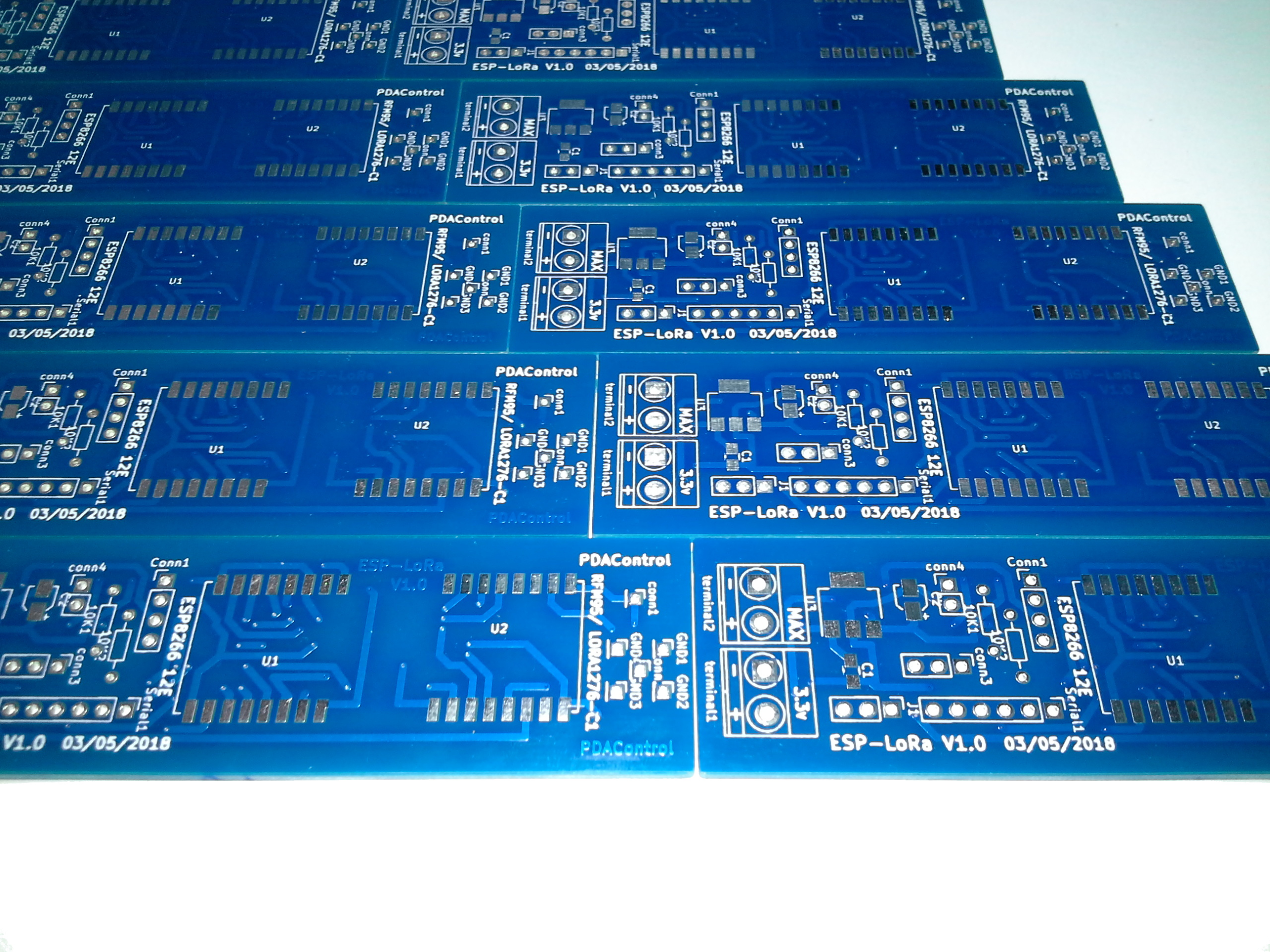
To Assemble Node / Gateway LoRa to be welded
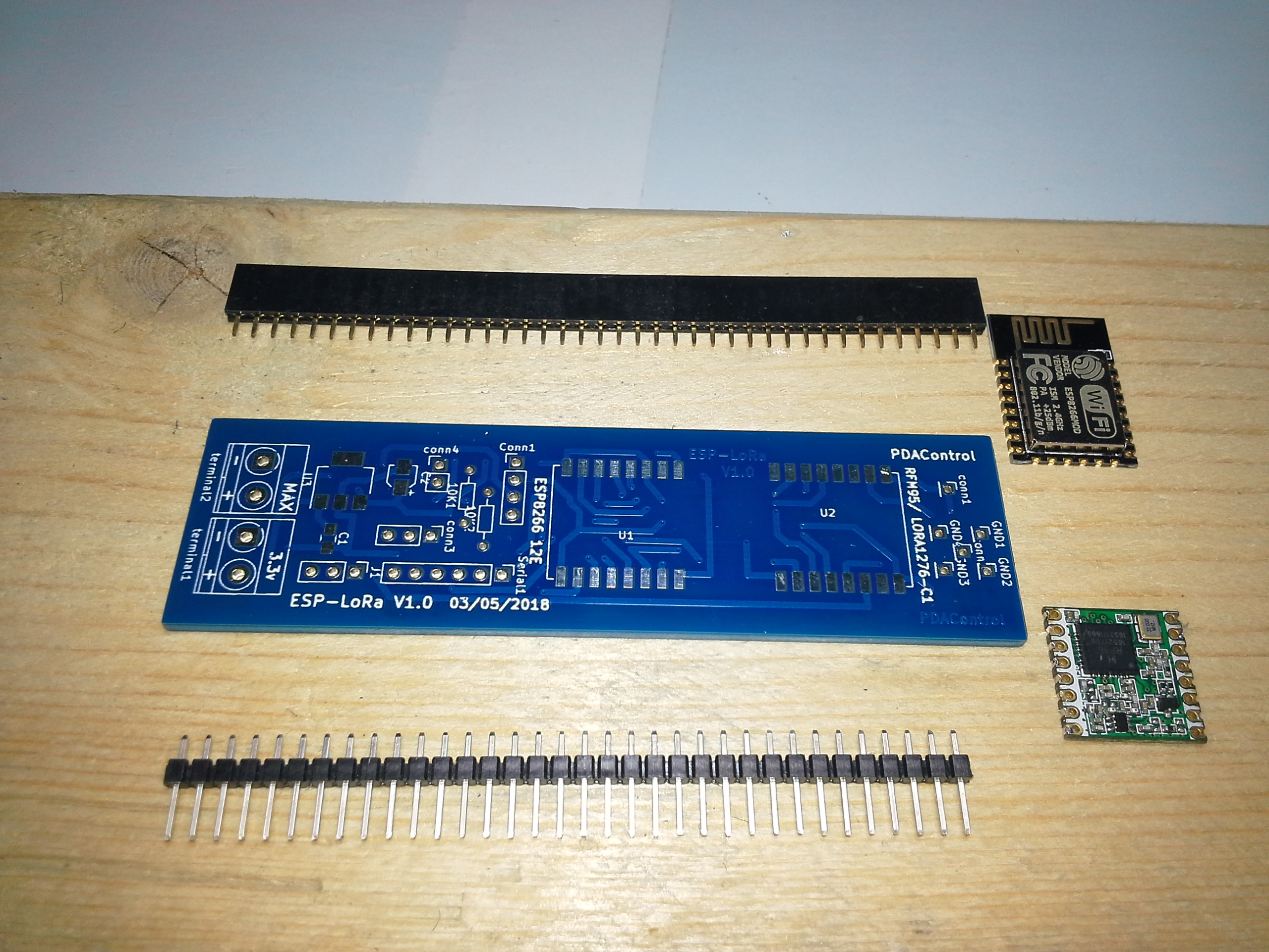
To weld ….
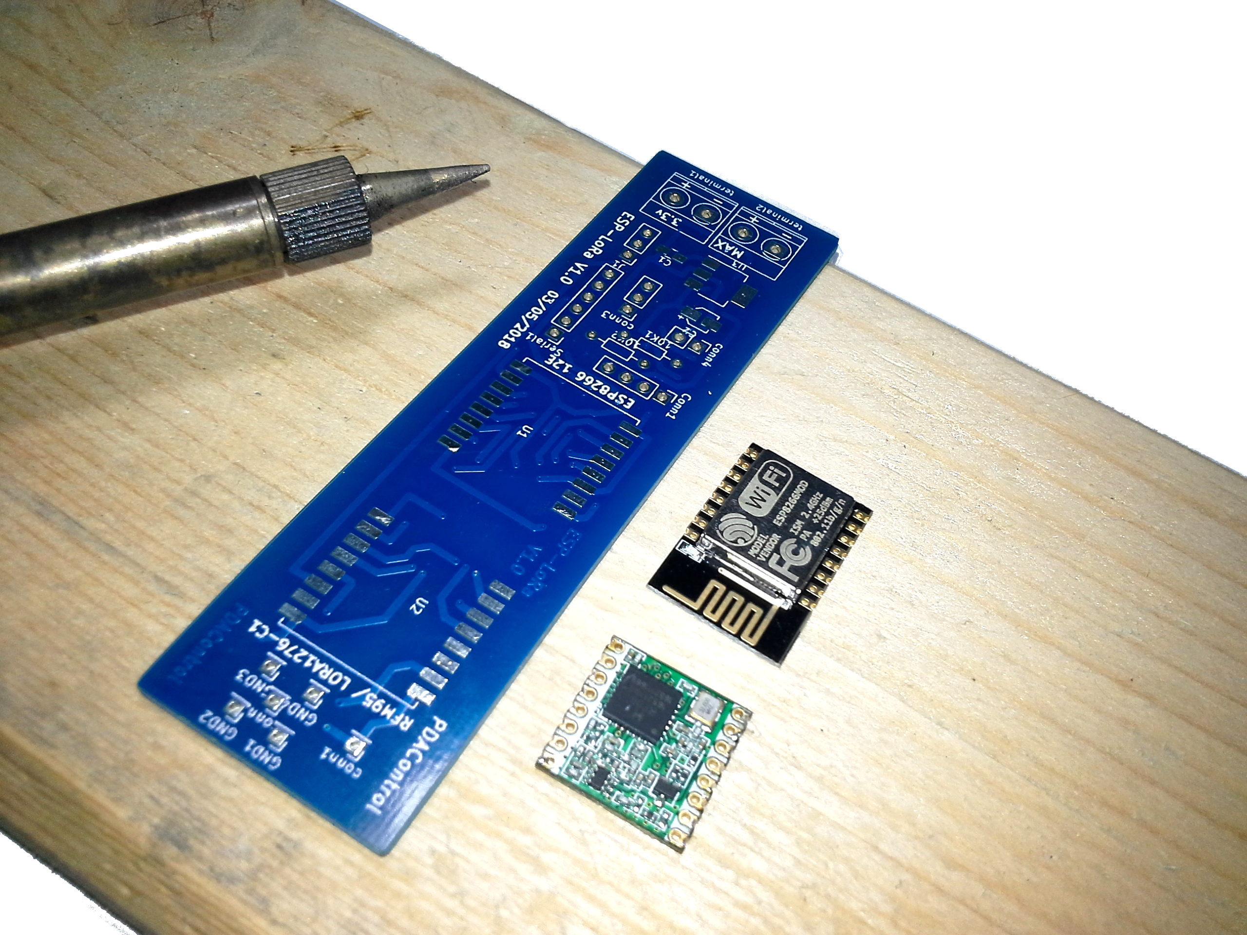
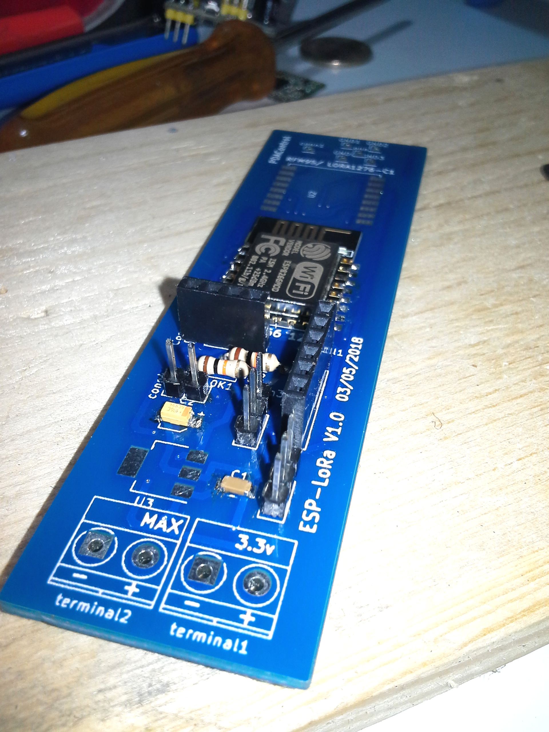
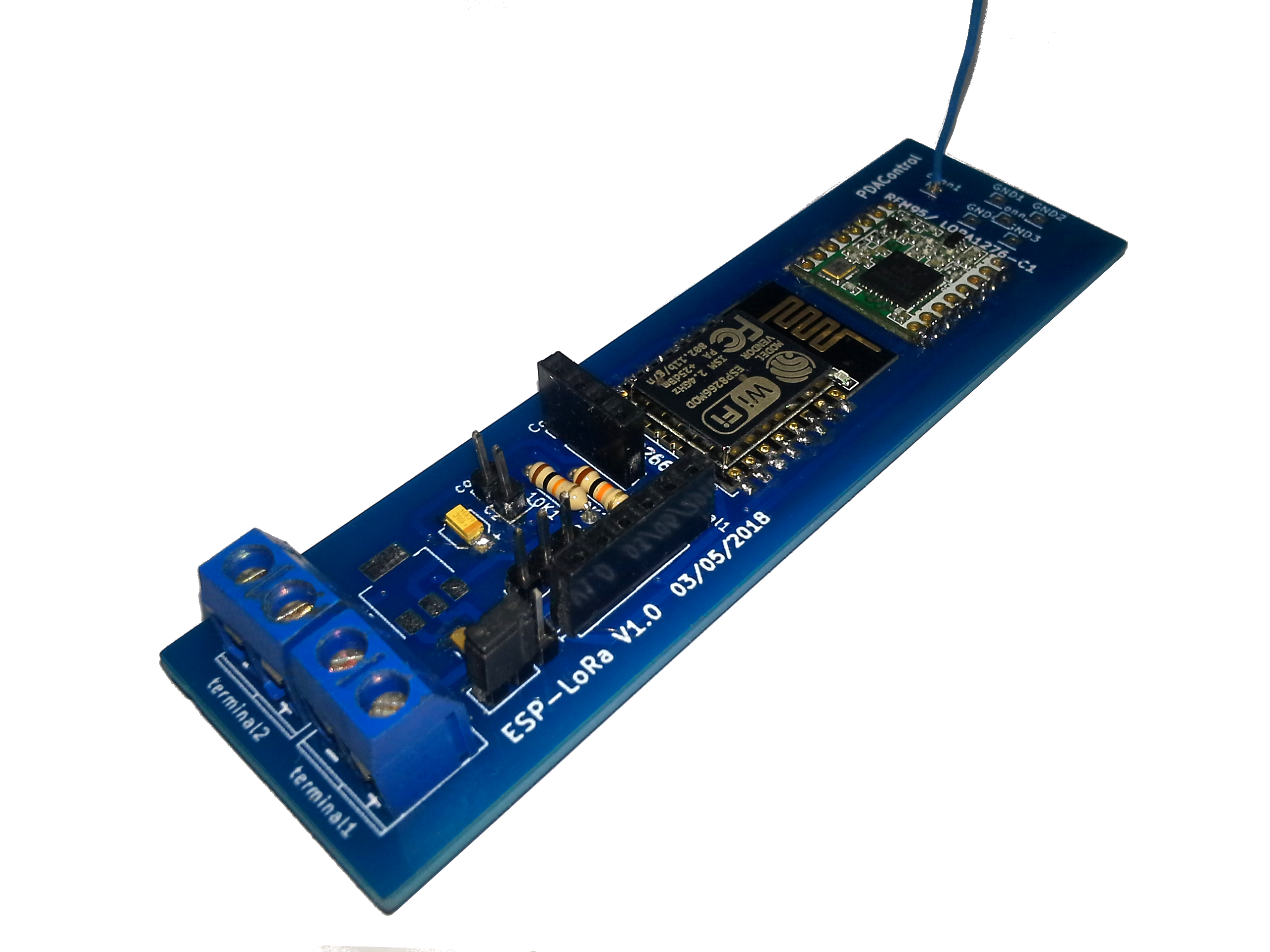
ESP-LoRa V1.0 Finished
Although all my components have not arrived, example regulators, I have already tried it and it works excellent !!!.
Video Tutorial Complete Step by Step
10 Prototypes PCB’S Esp-LoRa Easy !!! with SeeedStudio Fusion PCB
Communication ESP-LoRa V1.0 ESP8266 & Radio RFM95 #LoRa
Recommended Tutorial : LoRa communication test with ESP8266 (Transmission – Reception)
Conclusions
My experience with SeeedStudio,, I already knew their products regarding hardware and I made the decision to test their PCB manufacturing service and I trusted in the recognition of this brand and it turned out very favorable.
I like it is finished in blue similar to the Arduino Plates.
I think I had an error with the copper polygon because I did not stay in the gerber, only the tracks remained but even so the plates were excellent and work perfect in future tutorials will see them in action.
This is the first version of my ESP-LoRa or ESP-LoRAWAN, going from a breadboard to a quality PCB is gratifying that my applications will not only be small tests.
I recommend this service SeeedStudio.com
- Very good price 5 USD for 10 PCB’s.
- 100% quality guaranteed.
- Good delivery time: 3 days by DHL.
- Online purchase order “online”.
- Technical support, in case of something someone always responds to you.
References
Downloads
- Gerber ESP-Lora File V1.0
Note: Version corrected with copper polygon.
